Power Designs TP340a Knob Upgrade

My Power Designs TP340a bench power supply has a look and feel of quality stemming from its industrial design roots in the 1960s. Unfortunately, my supply was built in the mid-1990s and the design was compromised by the use of plastic knobs for the voltage controls on each of the three independent power sources.

TP340a with "original" plastic knobs.

TP340a with “original” plastic knobs.

Since getting the supply up and running, I’ve been on the look out for some suitable replacement knobs. Other/earlier models of these Power Designs power supplies appear to have used knurled aluminum knobs supplied by Kilo International. Kilo sells similar knobs to this day, but they apparently long-ago discontinued the model Power Designs used (which is probably the reason for the substitution in the first place).

In the current lineup, Kilo has two lines that might serve as suitable substitutes. The JD series has the right overall profile, with a flat top rounding into a straight side, but it lacks the flared skirt of the originals. The DDS series has the skirt, but the rest of the profile isn’t right, with a flat top dropping to a flat side that then flares slightly for the knurling.

I suspect that the original knobs were a skirted variant of the JD series, probably called JDS. I scoured eBay for old stock or used knobs, without luck, but I did find a seller with used knobs of similar design. In fact, they look like knobs that Power Designs used on a number of supplies made in the late 60’s or early 70’s. The price wasn’t bad either, 5 knobs for about $17, shipped.

They still weren’t quite right though. The fact that the design wasn’t an exact match wasn’t the issue. Rather, I was concerned that they were a little wider than the original knobs, and  that their proportions would seem off (I lack the skill to create a nice, well proportioned design, but I can tell when things are off). Because of this, I dithered on ordering them, but after seeing his stock decline, I finally pulled the trigger.

IMG_8866

The knobs were in pretty good condition, other than being a bit gunked up. I gave them a washing and scrubbed them gently with some Barkeepers Friend (a mildly abrasive cleaner for glassware and stainless steel) before replacing the existing knobs.

IMG_8859

I think my concern about proportions were warranted. The I think the knobs give the supply a bit of a big-nosed look. Still, I think they look better than the plastic knobs that it had before, and the definitely feel better to use.

IMG_8861

The seller also offered some knobs with the same design but a smaller diameter. I would have purchased them instead, but for the fact that they were drilled for small diameter potentiometer shaft. I considered getting them and drilling them out, but I don’t really have the right tools and so I figured it would be a frustrating project that I could do without right now.

EDC 521 Voltage Source Stability and Accuracy

IMG_8647

Last week, I cleaned up the used EDC 521 DC Voltage & Current Source I bought on eBay and ran it through some quick tests. The next day, I connected it up to one of my Keithley 2700 6.5 digit multimeters, started logging readings, and powered it up. Since then, I’ve been collecting voltage readings every 5 seconds so I could get a better sense of the device’s stability and accuracy.

The EDC 521 was set to 10.00000v and powered on.

to4hr

Once the self-tests ran the output turned on. The initial voltage was only 9.99954v, but climbed quickly. After 15 minutes, it was up to 9.99981v and still rising gradually. At the end of the specified two hour warm-up period, it was 9.99986v, well within the specified tolerance of 0.000258v (0.002% of setting + 0.0005% of range + 3uV), as well as the DMMs uncertainty of 0.000350v 30ppm of reading + 5ppm of range.

2to8hr

After the initial warm-up, the voltage continued rising for another 5 hours, before leveling out at about 9.99989v.

From2hr

The graph above shows the voltage over ~4 days following the two hour warm-up period. If we look at the stability once the voltage first leveled out ~7 hours after turn-on, we see that it lies between 9.99990v and 9.99994v, which works out to be about 4 parts per million (ppm), which is better than the specified 7.5ppm 8-hour stability and the 10ppm 24 hour stability for the source and ~14ppm 24-hour stability of the DMM.

I’d guess that some of the variation is due to temperature changes. The EDC 521 specifies a temperature coefficient of +- 5ppm/C°, and the DMM has a temperature coefficient of about 2ppm. Unfortunately, I didn’t start collecting temperature readings until yesterday afternoon. Once have accumulated a few days worth of readings, I’ll look at the relationship between temperature than the voltage reading.

last3hr-bounds

The last thing I did was look at short term variation in readings. The graph above looks at a 4 hour period earlier today. The blue line is a moving average of 10 minutes of readings (~120 readings), the dark green shows the standard deviation in readings over the same window, and the light green bounds the average of the minimum and maximum readings over the same period.

It shows that the difference between minimum and maximum readings are ~6uV, which is  less than 1ppm. The DMM is only a 6.5 digit DMM, which means that the smallest reading on the 10v range is 10uV. When readings are taken using the GPIB or RS-232 interfaces, it does report an extra digit, which is useful for statistical purposes. In this case, I think its safe to say that the short term variation in readings is probably mostly down to the DMMs noise floor.

After looking over this data, my conclusion is that I got what I was hoping to get, a stable and accurate precision voltage source. Next step is to test the GPIB interface and use it to collect data across every available setting and range to check for linearity/accuracy and decide whether any adjustments are needed.

New to Me: EDC 521 DC Voltage/Current Source

Last week I came across a miscategorized eBay listing for an Electronic Development Corp (EDC, now owned by Krohn-Hite) 521 DC Voltage/Current Source. It was listed in the network equipment section, with “Juniper” as the manufacturer.

The EDC 521 is a precision DC reference source with high accuracy, precision and stability, for the calibration of meters and sensors. It can output voltage in three ranges, (0-100mv, 0-10v, and 0-100v), and constant current in two ranges, 10mA and 100mA (with compliance voltages up to 100V). In each range, the precision/resolution of adjustment is 1ppm. Overall stability in Voltage mode, within the devices operating temperature range is 7.5ppm over 8 hours, 10ppm over 24 hours, 15ppm over 90 days, and 20ppm over a year. The temperature coefficient (which is included in the above estimates). It is microprocessor controlled and has a GPIB interface to allow remote control.

To achieve its basic stability, it uses an aged and selected 1N829 temperature compensated Zener diode as its primary voltage reference. This diode is driven by a stable precision current source at a current chosen to provide the best combination of temperature stability, long-term drift and low-noise for the individual diode used in each unit. Adjustments are made using a custom, precision 24-bit digital to analog converter.

Voltage divider resistors and 1N829a temperature compensated zener voltage reference.

The DAC works by feeding the reference voltage across a resistor divider to obtain 10 output voltages, tapped at 500mV intervals. If I understand correctly, these voltages are switched to provide analog voltages for each decade, these voltages are buffered, then then weighted and summed using some precision resistors before being fed to the output amplifier.

When the package arrived yesterday, I saw why the listing had been miscategorized — it was packed in a box for a Juniper Networks switch. That, and the sticker noting a failed calibration attempt in 2009 makes me doubt the seller’s assertion that it was “pulled from a working environment.” Not that I expected a pristine, calibrated instrument for $150.

IMG_8649

Inside the box, I found things in a bit worse physical shape than I expected. What I thought was shadow/glare in the photo from the ebay listing, was actually a torn red filter over the LED display. And the underside of the case, which wasn’t pictured in the listing, had a huge dent.

IMG_8625IMG_8643

On closer inspection, the dent didn’t reach the PCB inside, and I was able to remove the panel and hammer it out. Once inside, I found that everything had a fine coating of persistent dust. Hitting it with canned air shook some of it loose, but most of it remained.

So, I got to work rinsing it with a lot of isopropyl alcohol which I then chased off the edge of the board with canned air. After a few repetitions, the top and bottom side of the board were pretty clean. I then looked over both sides of the board closely, looking for damaged components, and cleaning out little pockets of residue.

I didn’t see any damaged components, but along the way noticed signs that the board had received some major revisions. There was an obvious bodge wire on the bottom of the PCB, but it was also clear that new holes had been drilled to receive additional components. On the top side, I found a cut trace, along with a couple of added resistors and a couple of capacitors. I haven’t traced everything out, but its obvious that the bodge wire connects to one end of the internal reference divider, and the rest of it is on the opposite end, so it would seem likely that its helping isolate the reference divider, and the voltages it produces, from noise sources.

It also appears that a number of power transistors have been replaced. Unfortunately, none of the components in question have obvious date codes, so its hard to guess when the modifications were done, and whether the transistors and the filters were added at the same time. Perhaps one of you knows how to decode the markings?  First line is a Motorola logo followed by “616,” the next line is “JE350,” which is the model/part number. The datecodes on other components pretty much all date to late 1996, and the MPU board has a label with the firmware revision and is dated January 1997.

Before closing it up, I took care of the loose plastic supports for the back-edge of the PCB, which holds heavy electrolytic filter caps for the power supply. I cleaned the old, crusty, failed double-sided foam tape off and replaced it with new tape so I could stick the supports to the back of the chassis again.

I powered it up, and gave it a quick check on all the voltage and current ranges. It seems pretty close to its 1 year tolerances. I was surprised by the amount of time it took to warm up and stabilize, but when I checked the manual, I saw that the warm up time is speced at 2 hours.

IMG_8648 IMG_8647

I powered it down over night. This morning I set up my computer to voltage readings ever few seconds and then powered it back up. I’ll post a graph once I have a days worth of data. After that, I’m going to write a script to run through all the possible settings and log the measurements. So, more to come!

HP 6114a Precision Power Supply First Look

I already have more working electronic lab equipment than I need, and more broken equipment than I can fix in the next month or so, but I still check eBay daily, and occasionally, I see a deal that is too good to pass up. This time, it was an Hewlett Packard 6114a power supply on sale for $75 + $19 shipping. The supply had been listed for $150, and I figured that if the seller was willing to cut the price in half, they might be willing to accept even less. I offered $55.

I’m really not sure what I was thinking. Part of me felt like getting the supply for $75 would be a great deal. Part of me thought that not getting it at all would be smart, since I didn’t need it, and had resolved not to take on other projects. Part of me wanted to see if I could get it for even less. In the end, it looks like the compromise I made was to try and serve all three, because I picked a price that was low enough that it might not be accepted, but high enough that I might end up with another piece of equipment. And so I did.

The HP 6114a was introduced in in the early 1970s and produced until at least the early 1990s. They typically go for something over $100 + shipping, so getting one for just under $75 would rate as a good but not great deal. From the photos in the listing, I thought I could make out enough of the serial number to tell that this example was made in 1981, a fact I confirmed once it arrived. It had the base single-turn potentiometer for the current control, rather than a 10-turn pot with a turn-counting dial, but I thought I could upgrade it myself for $10-20 in parts.

Physically it seemed in fair shape. There were some bent fins on the heatsink, and the front panel trim wasn’t seated properly, and might need to be bent back into shape. Most of the finish seemed to be in good shape. The condition of the front panel was harder to judge. It was hard to tell what was sticker residue and what was scratches in the finish.

The unit arrived from Nevada about three business days after I ordered it. It was packed in a stout cardboard box, and heavier than I expected. Inside I found it wrapped in a few sheets of thin foam, nestled in a reasonable amount of packing peanuts. I think there were enough peanuts to protect the instrument as shifted in the box transport, but I’m not 100% sure, because there was some damage to the front panel and its hard to tell if it was pre-existing, or it occurred during shifting.

HP 6144a Front Panel

There weren’t any big surprises after I got it unwrapped. Next step was to start taking it apart so I could figure why the top trim on the front panel wasn’t seated properly, and what I could do about it.

Along the way, I also performed an initial inspection of the electronics to look for damaged components, PCBs and interconnect wires.

I quickly spotted some damage to some of the pvc tubing used for cable management (above left). It looked like it had been scorched by an errant soldering iron, suggesting a previous repair. It took my a while to figure out that the site of the repair was (probably) right there in front of me. That a big resistor (above right) is not like all the other big resistors. It’s epoxy packaged. The rest are ceramic.


My deeper inspection showed that displaced top trim wasn’t bent, as I feared. The aluminum extrusion was in good shape, other some chips and gouges in the finish, some of which had cut into the underlying aluminum. With the top trim removed, I could take a closer look at the other components of the front panel.

IMG_8562

The meter was in pretty good shape, but its grey plastic bezel, which also served to help retain the clear plastic lens piece, was broken in the lower left hand corner. I removed the bezel and glued the crack with some superglue. Once it was dry, and sanded it down and polished it with some nail files/polishers I got surplus from my wife. The crack is still visible if you look closely due to glue filling in fit is repaired and the profile and finish of the plastic is pretty close to what it originally was.

IMG_8565

During initial inspection, I noticed a rattle as I turned the instrument over. As opened the chassis up, I was attentive to the source of the noise, but couldn’t pinpoint it. In the process of removing the meter bezel, I realized the loose part was in the meter. I desoldered the meter leads so I could inspect the meter more easily. As I did, the source of the rattle quickly revealed itself to be small screw and copper lock washer. Once I had the meter free of its leads, I removed a clear plastic clip holding the meter lens to the back of its housing and worked the lens loose. With it free, I could see the source of the loose parts, they were one of the pair fastening the printed meter dial to the frame of the brass meter mechanism. They’d somehow worked themselves loose.

The copper washer dropped out as soon as I opened the meter housing, but I lost track of the screw. It wasn’t on my workbench, and gentle tapping of the meter housing didn’t shake it loose. I went in search of a suitable tool for removing the recessed nuts at the back of the housing that hold the mechanism to the meter. The socket wrenches I had were too thick-walled, but a fine set of needle nose pliers ended up doing the job. I still couldn’t find the screw though. I pulled the internal leads free of the pins that passed through the housing so I could take a closer look. Perhaps the screw had found a spot inside the works of the mechanism? After 15-20 minutes, I concluded that it must have dropped out as I carried it in search of a wrench. After searching around on the floor around my chair for 10 minutes, I broadened my search area and almost immediately spotted it camouflaged in a dust bunny on the other side of the table, along the path I took to the basement to look for tools.

HP 6144 Voltage Control Sub-panel

After reassembling the meter, I decided to remove the one screw holding the voltage control subpanel to the chassis and take a closer look at it. That doesn’t look right, does it? That bow isn’t lens distortion, that’s bent aluminum. I can’t tell from the photos in the listing if the damage was already done, or if it happened in transit. One way or another, it looks like the result of sliding or being pushed face-first against something.

In preparation for repair, I desoldered the two leads connecting the voltage control to the main PCB. One connected into a PCB on the sub assembly and was easy to remove. The other connected directly to a lead on the potentiometer shown in the photo. It was a bit fussy. The leads from the pot are basically ~22 gauge wire with a hairpin bend at the end. To get the wire free, I ended up removing most of the solder with some desoldering wick, and then alternated between teasing the hairpin open and working the wire free. All in all, it was fussier than I would have liked, and I ended up scorching some of the plastic potentiometer housing when I accidentally touched it wit the side of the soldering iron. In retrospect, i should have removed the knob and unscrewed the pot from the front panel before trying to desolder the lead.

With the assembly free, I removed the knob and retaining nut on the potentiometer, then I heated the aluminum carefully with a hair dryer so it was easier to pull the thinner front sheet with the labeling free of the the thicker extrusion so that I could get to the screws holding the decade switches.

HP 6114a Voltage Control Subpanel Repair

With the bent extrusion isolated, I used a hammer and a few hardwood blocks to carefully beat it back into some semblance of flat. I think I did a pretty good job.

IMG_8569

I also spent some time cleaning the stickers and adhesive off the remainder of the front panel. I started by peeling off what I could, which revealed some writing with permanent marker. Isopropyl Alcohol on some cotton balls and a little elbow-grease took care of all the adhesive and faded the permanent marker.

I used an old “drafting” eraser to rub out the last remnants of the magic marker and a few persistent spots. I think its looking pretty good. There are a few tiny scrapes in the white panel, and a few more in the grey strip at the bottom that I think I’ll leave be. Some of the lettering on the white panel is a little worn. I might try touching that up.

IMG_8576

The most glaring problem is the missing HP logo badge that is supposed to fit over those two holes in the upper left of the panel. Given the vintage of this supply, I think the original logo badge had charcoal and gray with a chrome border. Anyone happen to have any spares?

Next step, I think is to put it back together and check to see how it works.


HP 6177C DC Current Source Troubleshooting/Repair

I picked up a Hewlett Packard 6177C DC Current Source on ebay for less than $75 shipped. This is a precision constant-current source that can deliver 0-500mA at up to 50V.

IMG_7318The seller described the unit as used with responsive controls and indicators. When I received it, I could see that while in generally good physical shape the upper right portion of the front panel was more bent/buckled than I could make out in the eBay photos.

So, first thing I did was partially disassemble the unit to fix the front panel.

Once I got it back together, I did some quick functional tests and found that the current output was consistently 1/10th the expected value. In the 500mA range with the current pot set to maximum, it produces a max of 53mA of current, on the 50mA range, it produces 5.3mA, and on the 5mA range, 0.53mA. This behavior doesn’t vary noticeably between shorting the outputs and having a 30 Ohm load. With a suitably high resistance, the voltage will hit >50v, provided the current doesn’t exceed ~50mA.

So, next step was to look at the service manual and work through the troubleshooting steps.

First thing is to check some voltage rails.  These all checked out, though a few were out of spec on ripple.

Next is to go through the problem isolation procedure, which starts with checking the guard voltage to see if it varies between 0 and -1V. Nope! In each range it maxes out at… ~100mV, or 1/10th of the expected value. Notice a pattern forming?

I started to work through the guard supply troubleshooting instructions, but I got hung up. After disabling the main supply, as instructed and checking a few voltages, it wasn’t clear to me whether I should go immediately through the subsequent steps, or reverse the change and proceed from there. Subsequent instructions just raised more questions.

I asked for guidance in the EEVBlog forum, and while waiting for a response, worked to better acquaint myself with the schematic and theory of operation of the device.

I’m still not sure what to do, and rather than pushing forward, I realize that I already have other incomplete projects that need my attention, I’ve gathered everything up into a bin and put this one on the shelf, for now.


Power Designs TP340A Continued and Concluded

An update on the Power Designs TP340A bench power supply I’ve been restoring and repairing. I started by replacing a bad Sprague electrolytic capacitor. While I was at it, I decided to replace all the big electrolytic caps. That didn’t go so well, because I put two of them in backwards and caused them to vent. After replacing the vented caps, I noticed that the supply wasn’t behaving quite right, and found that some key voltages were out of spec. After some trial and error, I figured out which components to replace to get everything in spec.

I was pretty pleased with myself, but the next morning I realized that I’d been too hasty to write off some drift I encountered while calibrating Source B. I started load testing Source A & B, both separately, and in tracking mode while watching the output on a multimeter, and my oscilloscope in roll-mode:

It didn’t take long before the voltage of the output on Soure B started a random drunken walk over the range of a 0.5v or more.  After a while, it stabilized again and I left it to run a few hours without incident.

Before turning things off, I started fiddling around, connecting and disconnecting things, varying the current and voltage, trying to provoke another excursion and before long, it did it again. I really wasn’t sure what was going on, and figured I’d need to consult the schematics and start a long process of trying to figure things out.

Lucky for me, over on the Eevblog forum, user nanofrog, who’d helped me pick out replacement capacitors, checked in on my progress and I shared what I just described above. He replied suggesting I look for thermal-related issues, like a bad solder joint. That made sense! I didn’t have any obvious problems when the unit was running, just when it was heating up and cooling down.

I spent a good chunk of my 4th of July indoors, in a warm, dimly lit room, abusing the PCB of my power supply with alternating blasts of hot air from a hair dryer and cold spray from an inverted can of electronics duster while measuring things with my scope and DMM. I also loosened mounting screws so I could flex the PCB. I wasn’t getting the dramatic results I was hoping for, but eventually, with enough persistence, I was able to get bad behavior by focusing my attention on the lower part of the board near C211. From the schematics, I could see that C111 had a role in damping feedback going to the main voltage regulating op-amp. I inspected the PCB closely looking for a bad solder join on this capacitor, or any of the components in circuit with it.

After a good hour spent squinting and angling to get a better look I hadn’t found an obvious problem, but I saw a few solder joints that I was suspicious of.  So, I heated up my soldering iron, daubed on some RMA flux and made sure I had some leaded solder handy and got to work touching-up the questionable joints.

Then I started testing it again. I repeated the cycle of heating and cooling multiple times without obvious problems. This morning I got up and did it some more, then left it running for a couple hours before calibrating it again.

This time, I didn’t run into any drift during calibration, but having declared victory prematurely once before, I wasn’t ready to call the project done. I needed more convincing.

Earlier in the troubleshooting process, I had noticed some subtler behavior when the PSU thermal equilibrium. All though Souce B’s voltage was stable from second to second and minute to minute under a steady current, it had poor load regulation, with changes of ~30mv or more when between 0 & 1A of current. Moverover, if I used the statistics function on my Keithley 2700 multimeter to take 1000 readings of the voltage while the unit was under a constant load, I found that the Standard Deviation in reads was 10x higher for Source B compared to Source A.

First, I checked load regulation of both Source A & B between 0 and 1A at ~10V. Both had a total swing of ~3-4mv. According to specs, it should be ~2mV. My measured values are worse, but not dramatically so, and also pretty similar between channels, suggesting to me that I’d managed to fix the major instability issue.

Next thing I did was take 1024 readings for each source with a constant load of ~1A, again at 10V. Both channels had a standard deviation of ~25-30uV, whereas previously, channel B would have been 10x. More evidence that I’ve indeed solved the major instability problem.

I haven’t checked transient response or ripple, or thermal stability or long-term stability, but  for the things I have checked, this PSU is very close to its original specs. Its also good enough for my purposes right now, so I’m going to call this project done and move on.

Power Designs TP340A PSU Troubleshooting & Repair

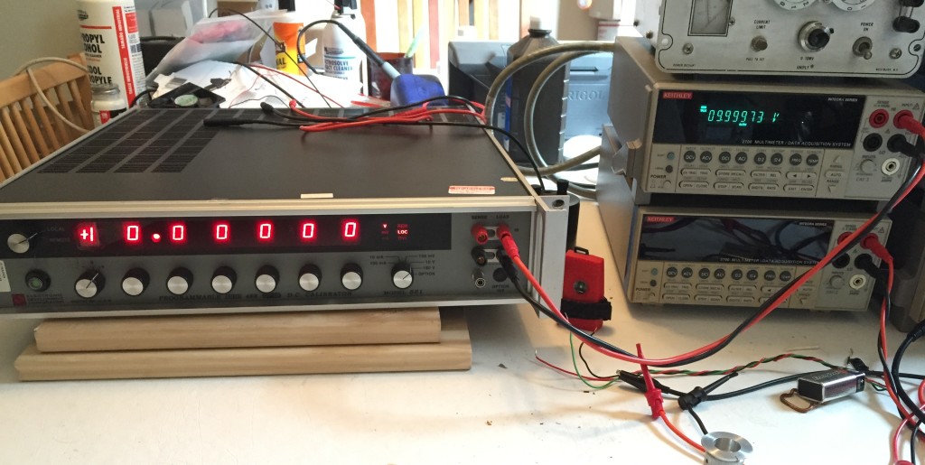
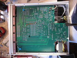
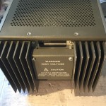
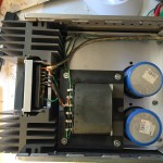
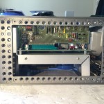
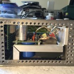
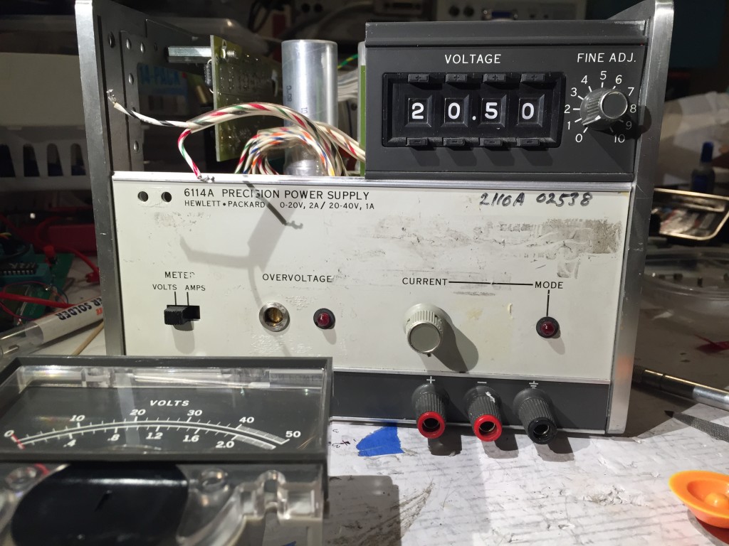
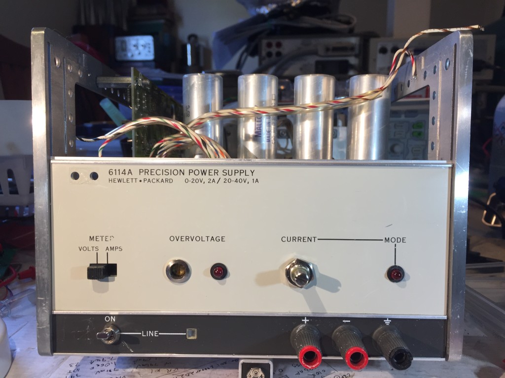
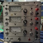
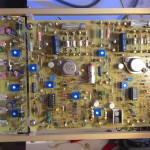
Previously I wrote about my clumsy efforts to refurbish a TP340A triple-output bench power supply I bought on eBay. The seller listed it as used, implying it was fully functional, but I was skeptical and opened it up to check it over. I found a bad electrolytic capacitor, and decided to replace all of them. In retrospect, I should have asked the seller for a partial refund, but I didn’t.

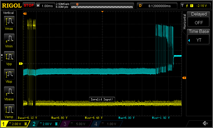
After I finished replacing all the electrolytic caps, things didn’t seem quite right. Source A seemed fine, but when Source B was set to track Source A, its voltage didn’t rise until Source A reached ~8V, at which point Source B jumped from ~0v to ~8v. It then tracked with Source A until reaching ~16V, and then started dropping off again.

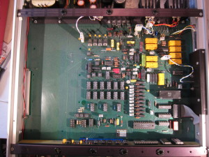
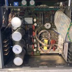
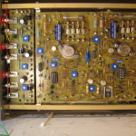
So I started working through the troubleshooting steps in the manual and checked the regulated B+ voltages measured on capacitors C104 (Source A) C204 (Source B), and C304 (Source C) are stable and fall within 12.4v DC and 13.2v DC.

B+ Voltage
Source A: 12.61v
Source B: 12.26v
Source C: 12.04v

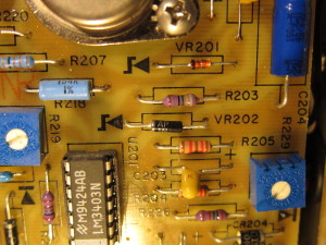
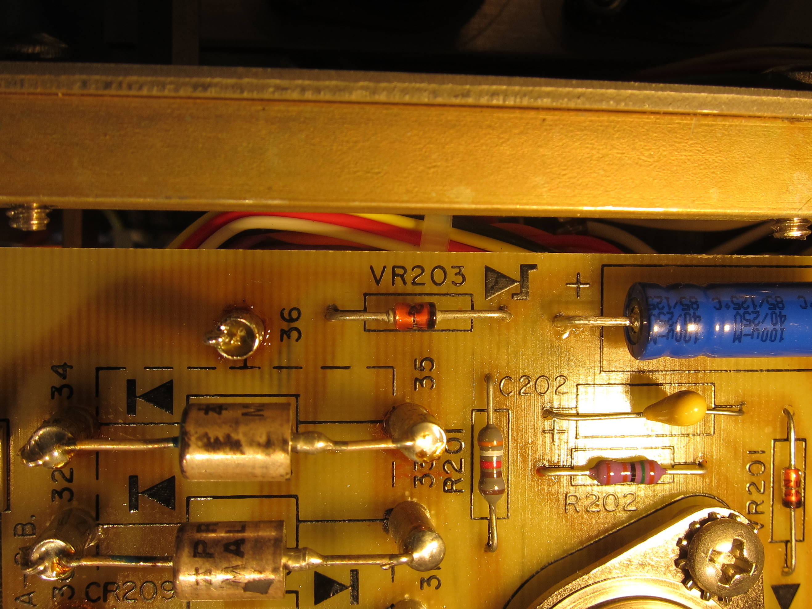
Clearly something wasn’t right, the values for Source B & C were out of spec. I continued by checked the voltages across the zener diodes VR103, VR203, and VR302 (nope, VR302 is not a typo).

VR103: 5.682v
VR203: 1.728v
VR302: 5.688v

Better here, in that two of the values are in spec (5-5.8v), but the value for Source B is WAY out of spec. Next steps, according to the manual, are to check for defective components, in order, capacitors C201-204, rectifier diode CR201, transistor Q201, VR201, VR202, VR203, and U101.

I’d already replaced C201 and C204, so I skipped that. I didn’t have great tools for checking components in place, so rather than starting to remove and test them, I first measured other components.

Main Source Reference Voltage

VR102: 6.31
VR202: 6.126
VR303: 6.010

These should fall between 6.26 and 6.52v. Only Source A is within spec.

VR101 5.629
VR201 5.639
VR301 5.619

These all check-out, falling in the range of 5-5.8v as they should.

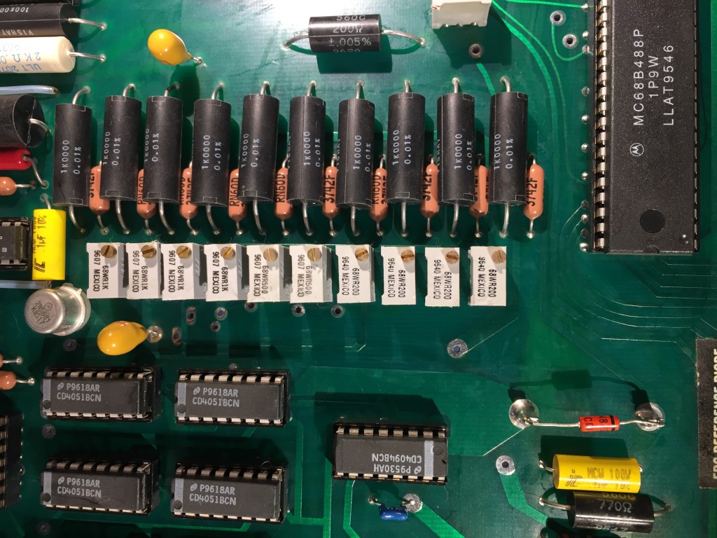
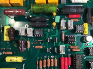
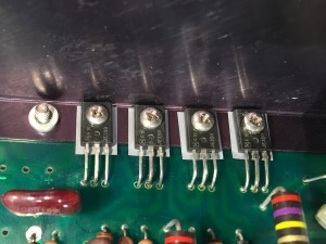
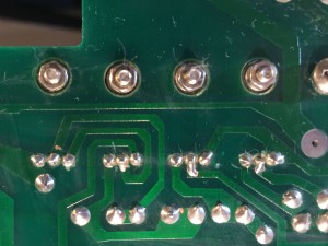
I lifted a leg on C202 and C102 so I could compare the values. I measured them with my AVRTransistortester with some test clips on leads.

C102: 1093nF, 6.9Ω ESR
C202: 1085nF, 1.0Ω ESR

Different, but different enough to be responsible for the other symptoms?  I didn’t have any idea, soo, I ordered some 1µF, 50v Kemet Tantalum capacitors and replaced C202 and C203 with them. The result?  No obvious change.
VR202

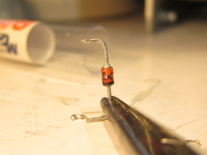
Next I wandered even further off the troubleshooting guide. I pulled VR202 to test it. As it turns out, I tested it to failure. No problem, right? Zener diodes are cheap and plentiful. I thought I probably had a suitable replacement in a semiconductor assortment I bought a few months back. Nope, nothing for that voltage. Time for another cycle of selecting a replacement, ordering it, and waiting for it to arrive.

Well, it turns out, selecting and ordering a replacement was a little harder than I expected. According the the manual, VR102, VR202 and VR203 are 1N825 zener diodes in grades G through K. Type 1N825 zener diodes aren’t run of the mill parts, they are part of a family of temperature compensated 6.2v zener diodes.

The family is made by creating a zener and a regular diode on the same piece of silicon in opposite orientations. In operation the negative temperature coefficient of the forward biased diode helps balance the positive temperature coefficient of the reverse-biased zener. The diodes are then burned in, characterized, and selected for appropriate temperature compensation. The 1N825 has a maximum temperature coefficient over its operating range of 0.002%/C. The family has the following temperature coefficients:

1N821: 0.01%/C
1N823: 0.005%/C
1N825: 0.002%/C
1N827: 0.001%/C
1N829: 0.0005%/C

There are also parts with the A suffix apply, which means they have maximum dynamic impedance of 10 Ohms, rather than 15 for the other grade. These were state of the art when they were introduced in the 60s, and have had a long run (my power supply was manufactured in the mid 1990s), but they’ve been superseded by other voltage reference designs.

In my initial searching, I only found references to 1N825A parts, not 1N825G, 1N825H, 1N825I, 1N825J or 1N825K, as described in the Power Designs part list in the manual. I figured they were probably proprietary Power Designs designations, but I decided to dig around more just in case. To help in that effort, I looked closely at the actual markings on the diodes. It didn’t help much.

AP
1N
825

The only new information was the “AP,” probably a manufacturer code, and the absence of the A suffix. My best guess is that the manufacturer code might be for American Power Devices, which manufactured 1N825 diodes.

In my wanderings, II found someone who claimed, based on experience, that newer 1N825 zeners had more problems with noise. At least, I thought I found someone who claimed that. I can’t find the source now. In any case, based on that, perhaps imagined, information, I decided to go looking for new-old-stock parts, rather than new parts from Mouser or DigiKey. I found someone on ebay selling Motorola-made military-spec 1N827 parts on ebay in lots of 4 for about $10 with shipping. Given my poor track record of ruining parts, I decided to buy 8.

VR102

With the new diode in place, I was back to where I started. Time to do the obvious thing and check VR203, the zener diode that was running at 1.7v, rather than the ~5.6 specified. The part number for this in the manual is 3EZ5.6D5. Without much effort, I found this number in an old Motorola diode catalog. Motorola’s spec is Glass, 5.6v, 134mA test, 500mW, 480mA max, and they cross reference it with the industry standard 1N5014.

IMG_7084

Time to check the actual part. I desoldered it to check it and test it. This time I avoided ruining the thing, helped, perhaps in part, by the fact that it was clearly already ruined. Time to figure out a suitable replacement.

IMG_7186

I checked the diode for markings. My eyes have gone downhill quickly in the last couple of years, so I deployed some optical assistance to determine that the diode was marked with the following.

1N
47
34
A

There was also a logo, which looked a lot like an older National Semiconductor logo. That made it a 1N4734A zener diode, not a 3EZ5.6D5 or a 1N5014. The 1N4734A is also 5.6v zener like the 3EZ5.6D5, but the test current is only 45mA. I ordered some NXP (successor to NatSemi) 1N4734A zener diodes from Mouser and, again, waited.

A few days later, the package arrived. I soldered the replacement zener into place, and plugged the PSU in, powered it up, and checked the voltages again. Success!  Source B’s voltages were now in spec!  On to Source C!

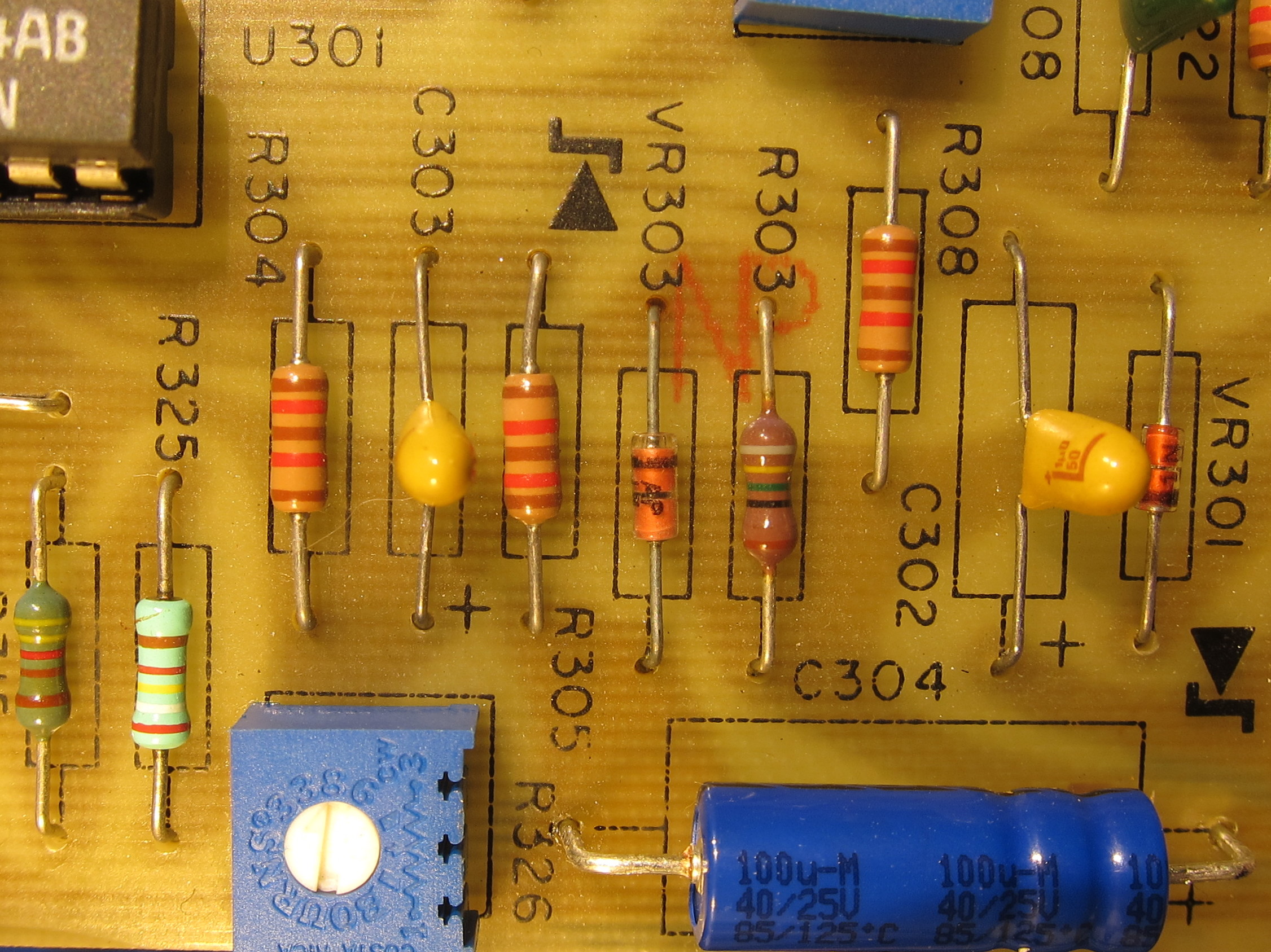
With source C, rather than checking caps and whatnot, I went right to the component that was out of spec, VR303, which had a voltage drop of 6v, rather than the specified 6.2-6.5v. First thing I had to do was double check the schematic to make sure I was looking at the right component. Most of the components in this section of all three sources have similar labels to the analogous parts in the other sources (ie C101, C102, C103) but for some reason, they broke this convention with the main voltage reference for Source C, VR303, rather than VR302.

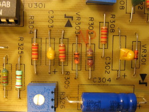
Apparently I’m not the only one who got confused. I had to check I was looking at the right  component, again, because while this was supposed to be a 1N825 like the others, it didn’t have the same thin black package and slender leads. In fact, it looked a lot like the 1N4734As I’d just dealt with. Once I pulled it out and got it under a magnifying glass, I saw that it was, indeed, a 1N4734A. I wonder who made the mistake? Most likely it was a botched repair.

Installed one of the extra 1N827s to fix the mistake, and decided to replace V102 as well, so all three channels would have similar parts of similar vintage and tempco for their main voltage reference.

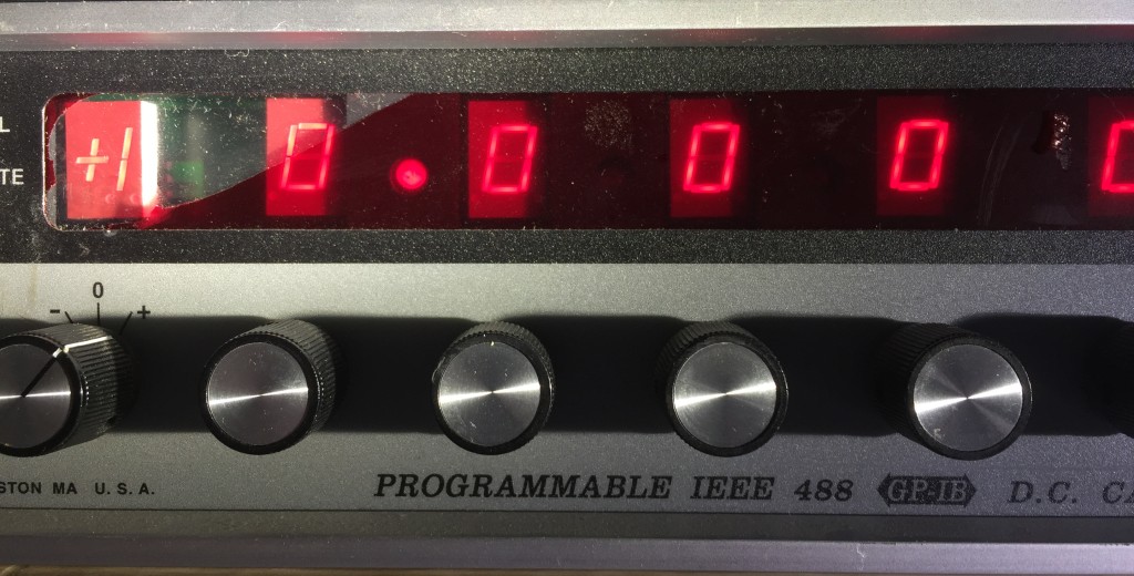
This time, when I powered it up, all the voltages were in spec. I did a little load testing and things seemed to check out. No more strange behavior with Source B lagging Source A in tracking mode, and it was able to deliver full voltage and full current on all channels. I moved on to calibrating the meters, adjusting the maximum voltage, and correcting the tracking offset.

I felt giddy, I’d fixed it! I was done, or so I thought. The next morning though, the sun woke me up early. As I was trying to fall back asleep I thought of something that had happened while I was adjusting the PSU the night before. I wasn’t done.
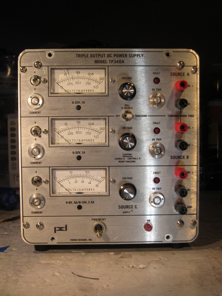
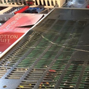
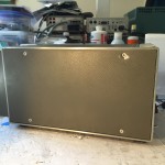
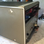
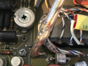
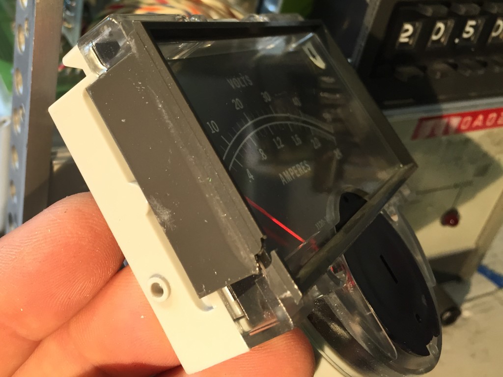
Power Designs TP340A Repair/Refurb

I picked up an old Power Designs TP340A bench power supply on eBay. The TP340A is a three channel (or “source) power supply. Source A & B have identical specs, providing up to 1A from 0-32v DC. They can be operated independently, or in tracking mode to provide positive and negative voltages. The third source only covers from 0-15v, but can deliver 5A at up to 6V and 2A at up to 15V. I bought it to power projects as I teach myself more about electronics. Little did I know what I was in for.

It showed up well-packed in great physical shape. There were a few scuff marks on the case where it had probably been pushed up against another piece of equipment, and some stickers and a few scuffs on the face plate, but otherwise, it looked nearly new.

When I took it apart, I found the insides were in similar condition.

On closer inspection though, I noticed something that wasn’t quite right

Bad C104 is Bad

The 100 uF 25V Sprague electrolytic capacitor in postion C104 looked like it had a bad inner seal. I decided not to power up the PSU until I’d replaced this cap.

The other two channels have the same type of capacitor in the same position in the circuit. They looked Ok, but I decided they should be replaced too, and while I was at it, I figured I’d also order replacements for the other big electrolytic caps. This decision proved to be a mixed bag.

The visually intact sibling 100 uF Sprague caps proved dead when I tested them after replacing them. On the other hand, the other electrolytics were still in spec. Which is more than can be said about some of their replacements.

After replacing all the caps, I powered things up and was greeted by a wretched buzzing metallic groan . I quickly switched the power off and gathered my wits, such as they were. Then I turned it on again for long enough to twiddle some of the knobs, things still weren’t right, but I had slightly more information. I switched it off again, thought for a minute, and switched it on again. This time the horible groan was joined by a ffffffssstPOPffffff. I switched it off, but there was another ffffffssstPOPffffff. I’d put two of the capacitors in backwards and they’d vented.

I replaced the vented caps with the originals getting the polarity right this time, so I could see if I’d done the thing permanent harm. Happily, the horrid groaning sound didn’t return the next time I switched the power on. It didn’t work though.

It didn’t take long to find them problem, I’d turned the voltage and current limit knobs the wrong way. After correcting that problem, I found that all the channels of the supply were fully functional, though things didn’t seem quite right. In tracking mode, source B didn’t respond at all until the voltage was up to about 8V and then started dropping off as it was turned up past 16v.

I started going through the troubleshooting steps in a PDF copy I’d found of the operating manual, but that’s going to be the subject of another post.

Keithley 2000 RS-232 Serial WTF

My Keithley 2000 DMM craps out during serial communications with a PC over RS-232.  When it does, the voltages on the TxD (yellow trace) and RxD (blue trace) lines look like this:

19.2kbps Fail KE

There are a few things wrong here.

  • The idle voltage of the RxD line should be -7v or so, similar to that of the TxD line, rather than the -1.7v it starts at.
  • The obvious decline in signal quality before the RxD locks at the ~1.2v shown at the end of the trace.
  • RxS locks at 1.2v, rather than returning to it’s idle voltage.

I came across someone who had trouble with the RS-232 level shifter IC on the similar Keithley 2015, so I carefully checked it out. It seems to be well under-spec on the output of its internal -10v power supply, which can only deliver a sustained 6mA. The +10v supply, on the other hand, can provide much more. I also diligently checking of voltages and current delivery of all the signal lines both the multimeter and the USB to RS-232 adapter its connected to.

It appears that the PC is trying to drive the RTS line to +7v. At the same time, the multimeter is trying to drive the RTS line down to -9v, and its loosing. As a result, it can’t drive the RxD line below -1.7v, and eventually, while transmitting, it gets stuck at +1.2v.

But why is the the DMM trying to do anything on the RTS line? That’s the job of the “data terminal equipment,” or DTE. I checked the reverse-engineered Keithley 2000 schematic, and it shows that the RTS line is connected to one of the transmit outputs of the level-shifter IC, something I confirmed by doing a continuity test. This makes no sense to me.

If I disconnect the DMM from the RTS line, everything seems to work fine. The DMM drives the RxD line to -9v at idle, and sustains signal quality throughout a transmission.

RxD is in much better shape when RTS isn't connectedI can’t imagine I’m the first person to come across this. I’m surprised though that I can’t find any mention of it online.

Update:

I posted about this in the EEVBlog Forums and a few users provided some details of similar issues they’ve had with RS-232 communications on the Keithley 2000 DMM. None of them have gone as deep as I have, but their descriptions are explained by my hypothesis.

I’m interested in whether later versions of the firmware leave the RST pin floating. So far no one with more recent firmware has checked for me, but one user remembers someone getting a similar problem fixed with a firmware update.

I’ll probably try doing a firmware update on my own. One user reports that he figured out he could use some Flash chips replace the EPROMs, which is attractive because I can re-use the chips and I don’t have to buy a legacy device like an EPROM programmer.

In the meantime, I picked up a straight-through male-to-female DB-9 cable and clipped off the RTS pin (#7). With it in place between the USB RS-232 adapter and the DMM, I ran a test querying the DMM with “*IDN?” every second for an hour or so. The DMM remained responsive for the whole time, and the responses it sent were complete, and uncorrupted. Previously things crapped out within a few minutes and only a few commands.

Update 2015-07-20:

I now have a unit from ~2007. It leaves the level of the RTS pin to the DTE, as it should. Upon closer inspection I found that the board has been revised so the RTS pin is no longer connected to the level shifter IC at all.

Keithley 2000 “Repair” Tip

I won an auction to buy a Keithley 2000 6 1/2 digit multimeter on Ebay for ~$250, a pretty good price. The seller said it had some scuffs, but was “tested and ready for work.”

When I received it, it was clear that it was a little worse for wear than claimed. It had a cracked rear bracket, and a yellowish/brown tint, rather than the shades of grey of a new machine. At first I thought it might be yellowing due to sun exposure, but the yellowing seemed to afflict the painted metal case as well as the plastics.

It did power up, and when I tested it with a voltage reference I have, its readings came in pretty close to the expected value, so I didn’t worry too much about the physical condition beyond trying to wipe the outside down well with cleaner and isopropyl alcohol.

Once I’d done that, I decided to look inside, to see if I could get an idea of the manufacture date. As soon as I removed the case, it was obvious where the yellowing had come from. It stank of old tobacco smoke on the inside, though fortunately, there wasn’t an obvious film. As I looked around, inside I could see a number of components with date codes for mid 1995, which matched well with the date of the first and only calibration, November 1995. It was almost 20 years old.

In the process of looking at the insides, I noticed that he input wires seemed a little close to some metal projections from the input selection switch, which seemed a little sloppy. Then I realized the board seemed a little slanty, and was out of its mounting tracks, possibly it had been jarred loose in an impact. On the opposite side of the chassis, I saw that some wires to the front panel and the power transformer weren’t routed through a retaining clip. Someone had taken this thing apart, and done a poor job of putting it back together. I loosened some screws so I could slide the board back into position and noticed a gouge in the PCB when it had been forced into place during a previous reassembly. Fortunately, it only damaged some solder mask, and not the trace underneath.

Once I had it back together, I ran the self-tests and was discouraged when it reported a number of faults for tests 100.1, 101.2, 101.3, 200.1, 200.2, 201.1, 201.2, 300.1, 301.1, 301.2, 302.1, 302.2, 303.1, 303.2, 304.1, 400.2, 401.2, 402.2, 403.2, 500.1, 500.2, 600.1, 600.2 and 601.2. That’s most of the self tests.

I tried to work through the troubleshooting in the repair guide, but it was dismal, it didn’t even describe the signals on the half-dozen or so test points on the board. I found a reverse engineered schematic and dove in.

I was working my way around the A/D chip trying to orient myself to the various signals, when I noticed…something. At first I thought it was a stray line on the silkscreen, but on a closer look, it seemed to be a fiber, cat hair? Dog hair? I flicked it away with my gloved hand, and then blew the area clear with some canned air.

I reran the tests and they all passed! One tiny fiber in the wrong place was enough enough to through the A/D converter out of spec cause a cascading failure.