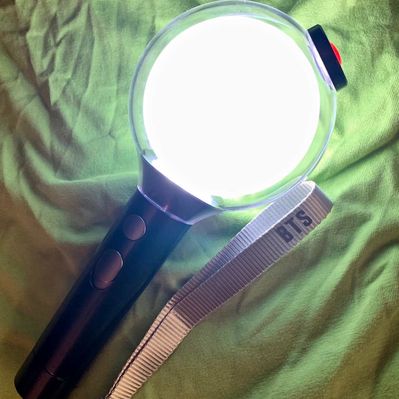
There was a discussion on the forum for the WLED firmware for controlling LED pixel strips about how the K-pop group BTS coordinates light-shows at its concerts using “Army Bombs.” Army Bombs are light-sticks that fans buy and take to concerts. They can be centrally controlled and used to put on huge stadium-wide light shows.
Someone in our house is a fan of BTS. They got an “army bomb” in preparation for a show in the US that ended up being cancelled due to COVID-19. I’m not allowed to disassemble it, but I was able to look at the label in the battery compartment and get the FCC ID and find their certification info.
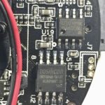
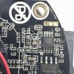
For some reason the internal photos are embargoed until 10/11/2010, despite the thing being in the wild. However, the test report reveals that it uses…BLE, which I already knew. It doesn’t seem to have another radio, though. I did find internal photos for a similar device, registered in 2016, from the same manufacturer. The markings on the bluetooth SoC aren’t legible in the photos, unfortunately.
I can’t find any real teardowns, but one fan took hers apart. No closeups, but its clear there isn’t an IR receiver anywhere IR could be received.
Some research into the present and near-future state of indoor locating technology led me, inevitably, to Bluetooth Low Energy (BLE) beacons. Bluetooth Low Energy led me, inevitably, into a short digression into Bluetooth “tags” for finding lost items like keys.
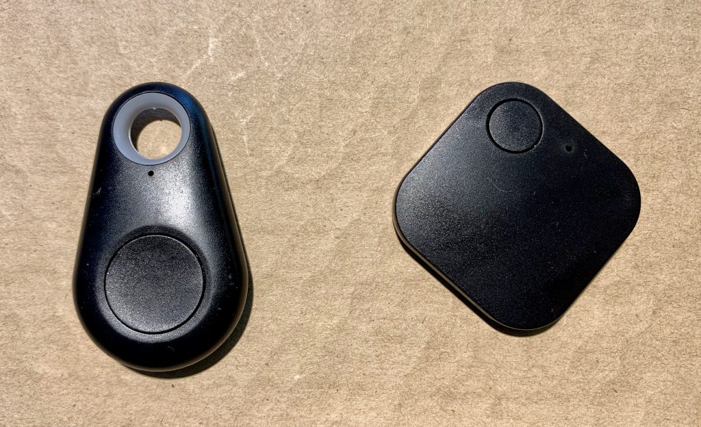
I just received a couple such tags I ordered from AliExpress for less than two dollars, each, and I made a video showing what’s inside when you open them up.
Yeah, I misspelled “bauble” in the title sequence.
These Bluetooth tags for finding lost items appeared on the market at about the time that Bluetooth Low Energy (Bt 4) started appearing in the latest smartphones. I don’t know who was first on the market, though I’ve seen the suggestion that the idea may have originally come from Nordic Semiconductor, one of the biggest companies dedicated to making chips for low-powered RF applications. I do know that Tile is probably the dominant vendor at this point.
The basic Bluetooth key finder “tag” is a small device, the size a condom packet, or a matchbook that can be carried on a keychain. Inside there is a small circuit board with a Bluetooth SoC (system on chip), a microswitch, battery, a pezioelectric speaker, and a few supporting components.
When it is powered on, the tag transmits to “advertise” itself. When it is advertising itself, a companion app, running on a smartphone can detect it and connect to it.
Once connected, the app periodically checks the signal strength of the tag. If the signal drops below a preset threshold, or is lost entirely, the app will notify the user, allowing them to stop what they are doing and find the object before they become too far separated from each other. The tag may start “chirping” automatically to make it easier to find. If the user needs help finding the tag while still nearby they can also use the app to instruct the tag to start chirping.
The system also works in the opposite direction. If the user is carrying the tag on a keychain in their pocket or purse, then the automatic chirping will warn them that they’ve become separated from their phone. If they realize they can’t find their phone when they are still nearby, they can also push the button on the tag to trigger a sound on the phone in order to make the phone easier to locate.
This basic functionality seems enough to be useful to people who loose track of things a lot. At this point, its available for less than $2, if one knows where to shop. For that price, one gets a functional but crummy app. The app may have added functionality, like the ability to use GPS to map the location where the phone was last able to communicate with the tag. This could be useful to determine you left your keys at the gym, rather than the office.
Tile, and others have gone further, in order to justify charging $20, rather than $2, and also to enhance their competitive position. If you use one of Tile’s tags, then, if your tag and your phone become separated, Tile’s app, working with their backend system, can check to see if any other Tile user’s phones “see” your tag, and then let you know where.
This tag-finding network sounds clever, but I wonder how well it works, and how useful it really is, particularly given the potential privacy concerns. It’s certainly possible to implement in a way that preserves privacy. In fact, Apple recently described the outlines of one such system they are developing to help people find lost or stolen Apple devices, extending their “Find My” app from iPhones to Apple Bluetooth devices, like AirPods, and also beyond WiFi range for Macintosh computers.
Apple is also rumored to be working on their own Bluetooth tag to allow keys and other objects to be tracked by the system. This might explain why Tile has recently partnered with a number of Bluetooth silicon makers, including Nordic, to extend the Tile network to third-party devices.
Back to the $2 tags I took apart, a few things of note:
The first has a teardrop-shaped case. The printed instructions point to the cTracing app. It shows up as “ITAG” using a general purpose bluetooth scanning app. Inside, I found a model XTR-FTQ-3432 PCB with V1.2, dated in 20181105. The SoC is from a Shanghai design house called Beken, and the part is BK3431.
Back in 2015, Brian Khuu tore down a tag that used the same case. His tag came, packaged for retail, in a box labeled iTag. Inside he found a different IC, labeled as ST17H25. One of the commenters identified it as a Telink TLSR8266 F512. It is actually a Lenze ST17H25. The two are quite similar, down to the names of the authors associated with revisions of the datasheet. It’s a bit overkill for this application, with a 14-bit ADC and, microphone input.
In any case, they’ve switched to a different SoC now. The BK3431 has a more limited I/O, making it more similar to the Lenze ST17H26, which is what I found in the second tag.
The second tag’s case has the shape of a rounded off square. There is a slot that a small lanyard can be looped through. Inside, it looks very much like the device pictured in this teardown on the Simply Soldered blog, which also uses the ST17H26 on a model RB-FD02 PCB. There have been some changes since then, though I’m not sure what they are. The PCB in my devices is V1.9, dated 20180606, the earlier teardown shows PCB V1.2, dated 20151212. I see some differences in component placement around the crystal and the antenna. I don’t know about accompanying differences in the schematic and if I took the time to check, and found some, I wouldn’t know the significance.
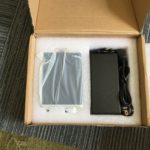
A couple of years ago I bought a Ravpower 30W USB PD powerbank with one USB Type-C port, and two regular 5v USB ports.
It was a little quirky. Sometimes it would start charging itself from the laptop until I held the button down for 5s. At some point the behavior started getting worse, to the point that last summer I left a poor review. The seller contacted me quickly, and I had a replacement within a week. The replacement fixed the problem.
That left me with the defective unit. Today, I decided to take it apart and see what’s inside.
Regulation of voltage and current for lithium ion battery charging for 1s-6s battery packs (4.2-25.2v)
Charging current to 10A!
Input voltage from 2.7-30v
Output to load from 2-30v & 60W
The pack sells for ~$75. To put things in perspective, you can buy eight FL1 cells for $4.41/each, which works out to about $35. That price drops to $3.56 each through a grey-market seller if you buy a thousand at a time. Ravpower is almost certainly paying less than that.
You can see more in the YouTube video I shot of the process:
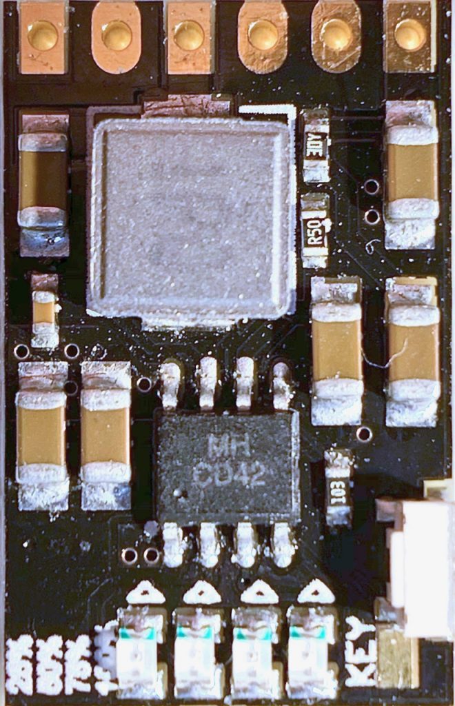
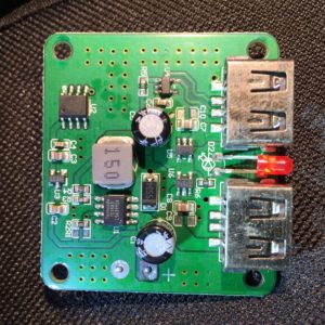
I just received a USB / LiIon power module I paid ~$2, including shipping, for on AliExpress. The model is given as MH-CD32 (link goes to what I think is the original manufacturer, though I purchased it from another seller with cheaper shipping).
The board is supposed to be an all-in-one solution for powering a 5v (ie USB powered) device from a lithium ion battery pack. I suspect the IC was originally designed for use in a USB powerbank. The basic features are:
Charging of 3.7v nominal, 4.2v max, lithium ion batteries.
5v charging input, 2.1A max charing current
Battery protection for over current, over voltage and over temperature (for the charging IC, at least, there is no provision for a thermistor to sense pack temperature)
5v output, up to 2.1A
4-level battery “fuel gauge”
Power path management: when the module is externally powered, it can power the load and charge the battery with any excess power from the supply.
Control input that can switch the output on, or off, suitable for control by a microcontroller.
100uA quiescent current.
It accomplishes this all with a single 8-pin IC, a dozen discrete passives (an inductor, eight ceramic capacitors, three resistors), four LEDs and a microswitch. All in all, it looks like a useful module.
I’m curious about what IC it uses. The package has markings, but they aren’t useful; it’s marked MH CD42, which is the model number of the module. Nothing strange about that, except that Google searches don’t turn up anything, no Chinese datasheets, just more product listings for the module.
Ordinarily, the first couple of letters of a chip marking echo the name of the manufacturer, but in this case, they instead they echo the name of the module manufacturer “MH-ET.” It isn’t uncommon that manufacturers “sand” the IC package to obscure it’s origin. In this case though, it seems that MH-ET has either remarked the chips or, more likely, had the packages custom marked.
If I were a competitor, and this were a product that had some combination of a large market, a high margin and a high selling price, I could go to great lengths to discover the true origin of the integrated circuit. I’d start by gathering the basic details of the product and using that to infer the specs of the IC. There isn’t much guess work in this case, because the product is a manifestation of the the capabilities of the IC, and its typical for the sellers to use the ICs specs when describing the module, even when the implementation cuts corners that may compromise the specs.
I’d use the specs I gathered to search catalogs and databases for similar ICs and compile a list of candidates. If my goal is to produce a competitive product in terms of cost and capabilites, I’d investigate pricing of the candidates and if any of them met the functional and cost requirements, that might be the end of it.
If I couldn’t find an equivalent chip, or if I wanted to improve my negotiating postion, or if I was involved in making or selling a competing IC, I’d dig deeper. I’d look more closely at the details of the IC, the specific package, the functions of each pin, the details of the circuit connected to each pin and I’d compare them to the documentation available for candidates I’d previously identified based on basic specifications.
Beyond that, I could order samples of the candidates and test their behavior against that of that of samples of the unknown chip. Or, perhaps I’d use chemical or mechanical means to extract the silicon ship from the enclosing package and then examine it under a microscope before and after stripping away layers of metalization on the IC. This might show me markings like a date code, part number, or logo. It would certainly show me the gross and fine structure of the circult. All of them would help me find the true origin of the integrated circuit.
I’m not going to do that though, in fact, I’ve already spent more time writing about it than I’d like to spend on what I am going to do.
Rather than going to those lengths, I’m going to take a shortcut that I happen to have available to me: I remember seeing a similar module on eBay a few months ago and I remember that the IC on that module had a distinct an unfamiliar manufactuer logo on it.
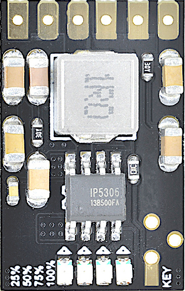
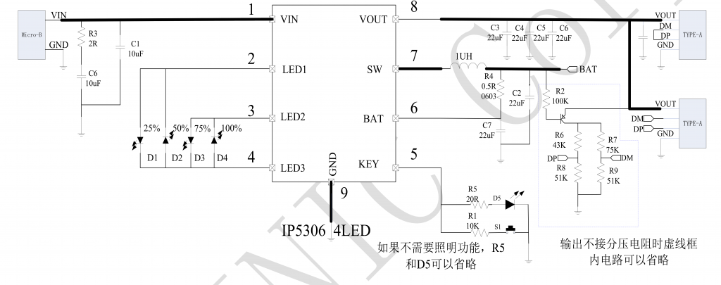
It took a little longer than I expected, but I found the ebay listing, or one like it. There IC lacks a distinctinve logo, but it does have a clear part number “IP5306,” and that part number leads to a catalog listing on a distributor’s site, a datasheet and the manufactuer, a company called Injoinic Technology.
The PCB layouts are very similar. The IC pinouts seem identical. I tried tracing out the circuit, but I could only get so far without removing components. The only real question are pins 6 & 7.
My 4.5 digit multimeter shows ~0Ohms resistance between them, suggesting they are on the same node of the circuit. However, if the IC on my MH CD42 board is the same or equivalent to the one on the IP5306, then those pins should actually be on two separate nodes of the circuit. Pin 7, on the left, should be connected directly to the near side of the inductor, while pin 6 should be connected to the far side of the inductor, by way of the low-value 500mOhm resistor you can see in the photograph.
IP5306 Typical Application Circuit
It wouldn’t be hard to pull off some components and replace them later, or it shouldn’t be, but I always seem to hit a snag on the easy jobs, like loosing a tiny component, or delaminating part of a trace. Fortunately, I have a nice Keithley 2000 6.5 Digit DMM. It’s serious overkill for most stuff, and measuring miliohms isn’t its forte, but it only took 30s to boot up (it actually has a Motorola 68030 process, like an old Mac ][, or SE/30 computer), and less time than that to show that the path from Pin 6 to Vbatt had 500mOhm higher resistance than the path from Pin 7.
So, my conclusion is that the MH CD42 IC is actually an Injoinic Technology IP5306. It’s possible that it is a “clone,” or that they both actually come from a third party, or are otherwise derived from the masks and foundry. It may also be true that there is another IC on the market that defined the specs and pinout and that a very narrow market niche has emerged around it. I already know more than I need to know, and if you’ve read this far, then you know it, too.
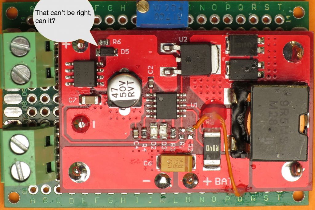
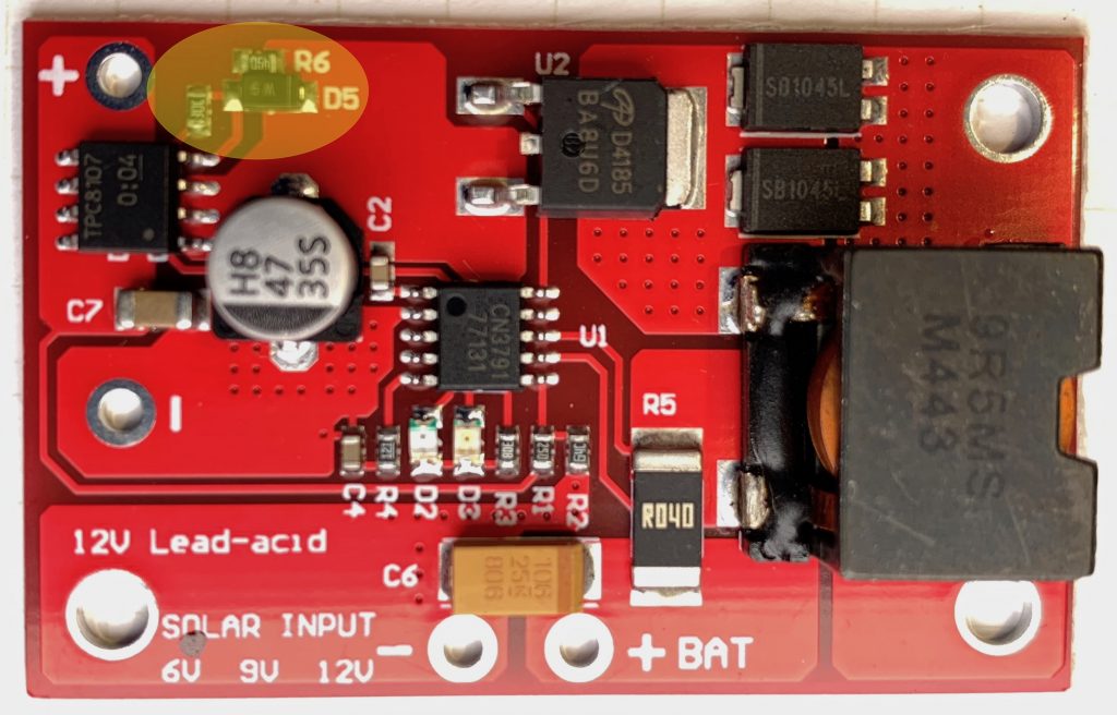
Last year, I paid about $3.66, with shipping, for this solar-powered MPPT lithium ion battery charging module on eBay to use with my small solar panels and scavenged 18650 batteries. It has some issues.
First off, the version I purchased/received is intended for 9v solar panels and I wanted to use it with a ~6v panel. This is set with a resistor divider. Careful study of photos from product listings showed that the divider was implemented using the same resistor value for the high segment of the divider, changing only the value of the lower segment’s resistor to change the setpoint.
The high segment had a value of 178KOhm and the low ranged from ~42KOhm for a 6v panel down to 12.6KOhm for an 18V panel. I didn’t have any SMD resistors of suitable value in my supplies, and I couldn’t find any I could scavenge on any surplus PCBs. I decided to use a trimpot instead. I had a variety on hand, and it would allow me to experiment on the optimal clamping voltage for the panel I had on hand, and an 18V panel I’d ordered. I chose a 200KOhm trim pot with the idea that approximating the total resistance of the existing divider would help preserve the stability of the control loop. If I were going to do it again, I’d probably choose a different configuration to minimize the impact of the pot’s temperature sensitivity. A simple choice would be ~20KOhm trimpot, configured as a variable resistor (short the wiper to one terminal) used it to replace the low segment, leaving the 178KOhm resistor in place.
After adding the potentiometer, I connected the battery and panel and adjusted the potentiometer until I maximized the charging current. I was a little surprised by how low the panel voltage was, and so I started poking around. The first thing I checked was the voltage drop across a P-Channel MOSFET on the panel input. I was surprised to find that it was 500mV, though knowing that, I wasn’t surprised the IC was noticeably warm. The panel was dissipating 1/10th of the panel voltage over the MOSFET!
Some of the photos on some of the product listings showed a simpler circuit, without anything in the panel input current path. My guess is that the MOSFET and accompanying resistor and diode were added in a revision in order to protect the circuit in case the panel polarity was accidentally reversed, and/or to block leakage of charge from battery through panel at night. A schottky diode would accomplish the same thing more simply, but with a voltage drop of ~300mV. Properly implemented, a MOSFET based “ideal diode” would have an effective resistance of ≥ 50mOhm, and a voltage drop of ≥ 50mV at the ~1A max current my panel could deliver.
I’m not completely sure how the circuit was intended to work, but clearly, it wasn’t doing the job. I wondered if it would work properly if I was using the module with a 9V manual, as intended, but that didn’t seem possible, either. The panel + was connected to the MOSFET’s source, the rest of the circuit to the drain, and the gate was connected to the drain via a resistor and diode. By my reasoning:
that the gate would ≅the potential of the drain
the voltage drop from source to drain should be as close to 0V as possible in order to maintain the efficiency of the curcuit
therefore, Vgs would/should approximate 0V
but it won’t because the Vgs threshold for the MOSFET was ~2V!
I wasn’t sure how to fix the circuit, but I was sure that the gate needed to be pulled down to a lower voltage, so I cut the trace connecting the resistor the drain and connected it to ground instead. It worked well enough that the voltage drop over the input MOSFET went from 0.5V to a trivial number. I’m pretty sure though that I didn’t fix the protection function.
I’ve since received another version of the module which has revised the input circuit. The diode and parallel resistor connecting the gate and drain are still used, but there as another resistor which connects to the charging indication pin on the CN3791, and in so doing. This pin is open drain. When the battery is charging, it is pulled low, lighting the charge indicator LED AND pulling the input MOSFET gate low. Vgs ≅ -Vpanel ≅ Vs ≅-6V, turning the MOSFET fully on.
Thinking through this further… if the battery is charged and the panel is illuminated the gate will approximate the potential of the input MOSFET drain and, since the only load on the panel is the quiescent current of the module, then Vsd ≅ 0V ≅ Vgs and so the MOSFET will be off, save any current through the body diode.
If the panel is dark and the battery is charged then Vd of the input MOSFET will, at most, be at battery voltage (Vbatt), Vs will be ~0v, Vg will ≅ Vd, Vgs ≅ Vd and the input MOSFET will be off.
If the panel is reversed Vs will be below GND and well below Vg ≅ Vd ≅ Vbatt so Vgs will be Vbatt + Vpanel, and the MOSFET will be off. Note: This means that reverse polarity with an ~18V nominal panel would exceed the Vgs maximum of 20V for the TPC8107 MOSFET used at the input.
If I get around to it I’ll draw a schematic and add it to this post.
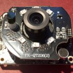
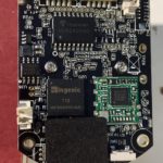
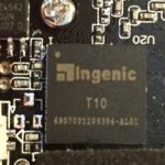
I was just looking at unfinished posts and noticed that I’d taken, but not published, a bunch of notes I’d made earlier this year in hopes of hacking better firmware onto the Digoo BB-M2 WiFi PTZ Security Camera.I gave up on the quest, but here are my notes, with minimal editing.
Someone mentioned that the Chinese language page for Netcam360 has a link to the IPC-SDK. When I downloaded it and looked inside, I saw client-side code, but there was also a self-extracting archive called “HSmartLink Win32 SDK” and I remembered the PCB marking started with “HSL.” Searching for HSmartLink brings up hsmartlink.com, which, among other things, has IP webcams! The i9812 looks like a good match for my camera!
Unfortunately, no sign of any firmware updates. I checked the .cn version of the site too. It doesn’t seem as up to date on products (i9812 isn’t listed), and while there is more info in support section, it is still quite sparse. Page that looks like it is intended to link to downloads hasn’t been updated since 2015
Company is “Shenzhen Hsmartlink Technology Co. Ltd”
So what is the relationship to NetCam360 (check whois & IP ) and they mysterious APKLink?
Nmap Pobe
Starting Nmap 7.40 ( https://nmap.org ) at 2017-02-06 18:38 PST
Nmap scan report for 10.31.1.124
Host is up (0.0043s latency).
Not shown: 998 closed ports
PORT STATE SERVICE
23/tcp open telnet
81/tcp open hosts2-ns
MAC Address: E0:B9:4D:8F:61:6C (Shenzhen Bilian Electronicltd)

Nmap done: 1 IP address (1 host up) scanned in 0.49 seconds
2.4Gh 1t1r 802.11n WiFi adapter chip. U-Suffix indicates USB2 Interface But it also refers to an efficient DMA engine and accelerators that offload the host processor.
I picked up a 21W, 3-panel Balight folding solar panel-based USB charger from Amazon for ~$36 a couple of weeks back. It uses high-efficiency SunPower Maxeon cells much like similar 20-21W panels from Aukey, Anker and dozens of obscure brands. All of them have the same basic construction. They are all made from nylon ballistic cloth. Each fold has a panel made from two SunPower cells encapsulated in a flexible waterpoof sheet. The panels provide power via two 5v USB ports, which presumably have some sort of voltage regulator.
I wanted to know more about how the chargers worked. In particular, I wanted to know if they were wired in series, or parallel because I wondered if it was worth trying to tap into the raw output, before the USB regulator to reduce power conversion and resistive losses for some applications.
I thought I’d be able to get the information I needed by finding someone documenting a teardown of their own panel on YouTube or a blog post. Despite the dozens of variants from dozens of brands and a handful of manufactures though, I didn’t find what I was looking for.
So, I decided to dig up a seam ripper and open my panel far enough to get a look at the wiring, and tap in to it upstream of the voltage regulator.
Bad photo of wiring
Another bad photo of wiring
USB Charger Output PCB
Backside of PCB
The panels appear to be wired together with some sort of woven wire conductor. I had some hope that all the cells would be wired in series, to give a nominal panel voltage of 18v. Based on what I could see, and measuring the voltage before the regulator in full sun, it looks like each panel is wired in series, for 6v nominal voltage, and then the panels are wired together in parallel. I was disappointed at first, but this arrangement makes sense in upon further thought.
Using a 2s3p configuration means that the input voltage into the switching regulator should be pretty close to the 5v (actually, 5.2v with enough sun and a light enough load) output of the USB power regulator, which will typically have higher conversion efficiency than 12 or 18 volts. It also means that the manufacturers can stock one converter for everything from a 7W single-panel charger, up to a 28w 4 panel charger without the converter having to support a wide range of input voltages. Perhaps most importantly, it means that partial shading of one panel shouldn’t have a disproportionate impact on the power output of the entire array.
The only downside is that resistive losses in the cabling will be higher with lower voltage and higher current, but that the interconnects aren’t more than a foot or so, the resistive losses shouldn’t be too high.
As for the converter itself, I may look at it more closely and add some more details, but, a few initial observations:
The PCB design has extensive ground planes on top and bottom, tied together with vias.
Both outputs are served from a single buck-converter (step-down) power supply based on a Techcode TD1583, which is a 380 KHz fixed frequency monolithic step down switch mode regulator with a built in internal Power MOSFET.
It looks like only port 1, at the top right in my photo, has the data lines connected, which suggests that it is the only one with fast-charge coding.
IC U2 looks like it has its markings sanded off. I notice though that one of its pins is connected to the enable pin on the TD1583, leading me to think that it is responsible for cycling the output to make sure devices draw as much power as possible when the panel voltage rises again after clouds or an object reducing the light falling on the array pass. I don’t know if it is a MCU, some sort of timer, or comparator, or what, though.
There you go. I can’t be sure that other folding solar arrays like this one are wired in the same way, but if they only support a 5v output, I suspect they will be. I hope this proves useful to someone besides me.
After ordering it, I was a bit worried I’d been scammed, because the seller never provided any tracking information, but those fears were quickly laid to rest when it arrived on my doorstep all the way from China in just 9 days!
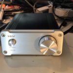
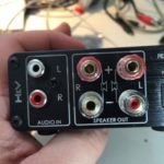
The TDA7492 chip is used in a lot of compact, inexpensive audio amps made by various Chinese manufacturers and sold under various names on Amazon, Ebay, AliExpress, etc.
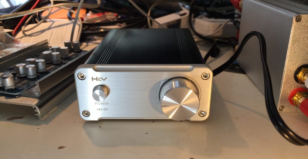
One such amp is/was the very similar looking SMSL SA-50 amplifier, which puzzled me, because when I first found the HV-50 listed on AliExpress, the seller listed it as an SMSL product. It wasn’t until I had it in hand that I realized that the eBay listing didn’t mention SMSL and there was actually no reference to SMSL anywhere on the product, or or the very thin users manual.
With some digging though, I found persuasive evidence that H&V is/was a new brand from he same company that produced SMSL. Given the price point, and product photos of the HV-50s internals, which showed signs of cost cutting, I assumed the H&V line would be a new, lower cost line, as SMSL seemed to be moving upmarket. Positioning the HV-50 as a lower cost alternative to SA-50 or A2 amps made sense when the HV-50 sold for $35-40, while the SA-50 & A2 were selling for roughly twice that. It makes less sense with the HV-50 selling for almost $60.
Looking more closely, the SA-50 seems unavailable from Chinese sellers on AliExpress and eBay these days. On Amazon, it sill goes for $60-70. The HV-50 seems to be in the process of being superseded. Aoshida, the source of my original amp seems to have both an eBay and and AliExpress presence. On AliExpress, they have a listing that pictures an HV-50 with a 24v power adapter for $42.28, shipped, but the listing is actually for a “TOE F1 TDA7492 amp” and notes that the housing may say HV-50, but it’s been “upgraded to TOE F1.” Their eBay store has a very similar listing, also for a “TOE F1 TDA7492 amp” for $53.00.
I think the HV-50/TOE F1 is a pretty good deal at $42 shipped with a power brick. At $50-60, that’s less clear. I’d probably pay another $10-15 for an SMSL SA-50. The reason? If the SA-50s shipping today are the same as those shipping a year ago (not a sure thing, given that SMSL changed the guts on the SA-36pro without warning, explanation, or acknowledgement) then they use some high quality film capacitors in key parts of the audio path.
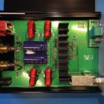
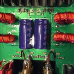
On the other hand, the HV is clearly a cost reduced design, as I suspected from the initial product photos, and confirmed upon receipt. It uses SMD ceramic caps for all but the main power supply caps. I personally think the cheaper caps work well enough. I don’t have an SA-50 to compare the HV-50 to, but while it’s possible they would sound obviously different, I doubt the SA-50 sounds noticeably better. For $30 less than the SA-50, I think the HV-50 is an obvious choice for those on a budget. For the current $10-15, price difference, it is much less clear cut.
What remains to be seen is if the TOE F1 is actually an upgrade, and if so, in what way? Will they adopt the film caps used by the SA-50?
Impressions
When powered up, a tiny click may be emitted from the connected speakers.
I noticed no obvious defects in sound quality. My main complaint is that the design & construction of the PCB-mounted RCA inputs doesn’t make good solid contact with the slotted, machined pins on some higher-quality RCA plugs, leading to noise or audo drop-outs. At first, I though the volume control pot was going bad. I ended up replacing the jacks with some gold-plated panel mount jacks with better design/construction. Interestingly enough, while the original part has trouble with higher-end RCA plugs, it has no problem at all with inexpensive stamped & rolled RCA plugs.
Speaking of connections, the speaker output binding posts are small, but work well with banana plugs, spade connectors and properly trimmed and stripped speaker wire (to avoid shorts).
Caveats
There are a few important caveats about the HV-50, which may or may not apply to the TOE F1:
First, it’s important to understand that the generation of class D amplifier chips like the TDA7492 used in the HV-50, along with the more powerful TDA7498, and the comprable TPA3116, all have consistently inflated power ratings. These ratings are often used in the specs of cheap amps built around such chips.
The inflated ratings aren’t exactly inaccurate, its just that they only apply under unlikely listening conditions. They assume a power supply voltage near the top of their operating range which ends up being 24v for the TDA7492 and TPA3116. This isn’t an issue with the HV-50, which comes with a 24v supply, but can come into play when using ~19-20v laptop adapters. The tests are often performed with ~4 Ohm loads, while lots of home audio speakers are closer to 8 Ohm, and peak power output would be ~50% of the advertised number. The finally issue with the ratings is that they allow up to 10% distortion, a value that most people will find unlistenable. Values are generally also given for up to 1% distortion, which most people will find suitable. The corresponding power ratings are ~50-60% of the advertised value.
In sum then, the usable power of the HV-50 and similar amps with a suitable power supply is 50W * 50% (for 8Ohm speakers) * 60% (for reasonable distortion levels), which works out to 15w/channel. This may seem much less impressive, but it should be enough power to push most consumer bookshelf speakers close to their (and your) limits.
Second, the HV-50 does not, as claimed in the Bangood listing and elsewhere, contain parts from EPCOS, Philips, ALPS, DALE, etc. The volume control pot seems like a cheap, but adequate generic Chinese part, and the capacitors in the audio path are all SMD ceramics.
Conclusion
Bottom line: The HV-50 is a decent, inexpensive Class D amp if you can get it shipped with PSU for ~$40. Whether it is a good choice vs an SA-50 or similar really depends on the price difference at current market prices.
Photos
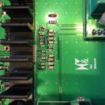
And finally, the main purpose of this post wasn’t writing a wall of text, it was sharing photos of the guts of my HV-50.
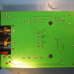
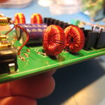
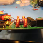
I’ve ended up with five small, inexpensive ($7-15 each) routers, running OpenWrt and only really need two of them, so I’ve been thinking of ways to use the others. One of my ideas was to get an external USB DAC, install Shairport-Sync, and use it as an AirPlay receiver for my car stereo, eliminating the need to connect an audio cable to my phone, and avoiding the mediocre sound quality of Bluetooth audio. It hasn’t quite worked out that way though…
While looking for an inexpensive (>$20), compact USB DAC with reasonable quality, I discovered there were integrated commercial products that already do what I planned to do. I already knew there were Apple-approved MFi-certified devices, but they tended to be expensive. I discovered there were cheaper devices using Shairport, but they tended to start at $30+.
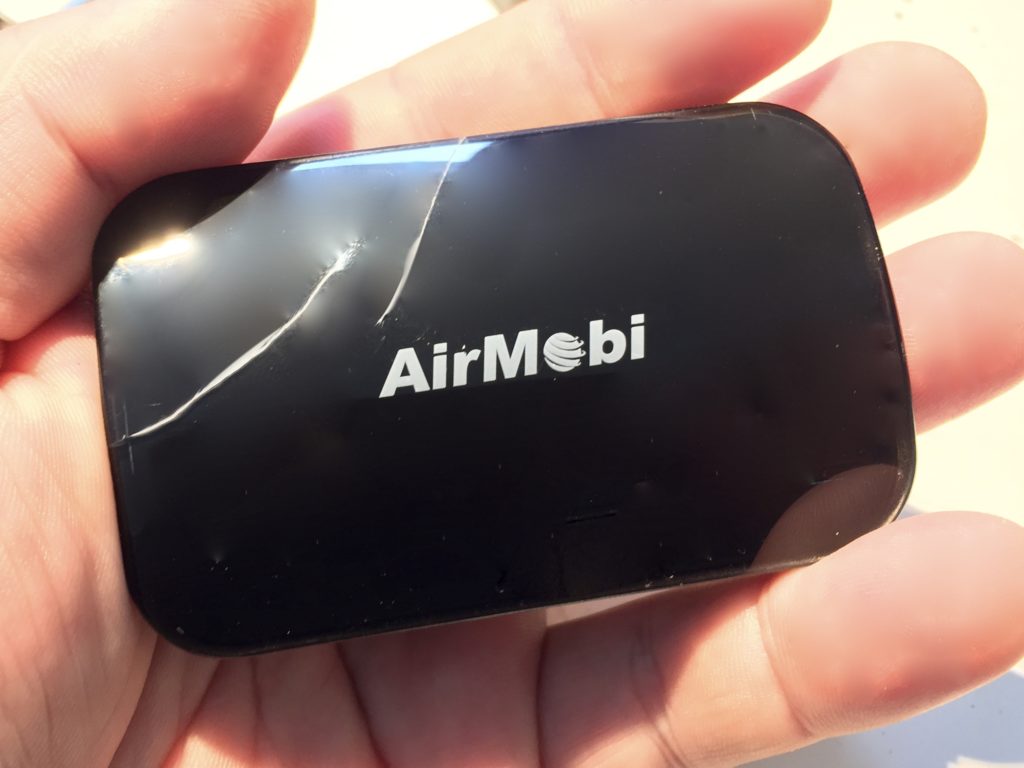
Damaged while trying to open the case.
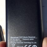
With a little more digging though, I found a device called the iReceiver, from AirMobi that sells for as little as $12!!!. According to the scant marketing materials, it has a 24-bit Wolfson DAC. I was surprised I couldn’t find anyone who’d opened one up to see what was inside. I did find an Amazon review from someone complaining that the usb power connector had broken off on theirs, and the included photo showed it had a Ralink RT5350F WiFi SoC, which gave me hope that it would be hackable. So, I bought one.
Before opening it up, I tried it out. It works as promised. It defaults to broadcasting an unsecured WiFi network. Once connected, it shows up as an AirPlay receiver in iTunes, etc. From there, you can connect it to some powered speakers, select it and start playing music. The audio quality doesn’t suck (no obvious noise, clipping, or distortion), and in my limited use, there were fewer dropouts that I’m used to with Bluetooth.
Beyond that, there are various configuration options available through a browser based interface. There are no audio-related settings at all. Most of the settings are networking related. You can rename and secure the WiFi network with a password (good), WPS (bad) and by limited connections to specific devices by MAC address (meh). You can also connect to an existing network (good), and, optionally, extend it (meh). This seems like a good point to mention that it also works as a DNLA “renderer” (DNLA is a more open standard than AirPlay, making this useful to Windows and Linux devices, and Android phones with an appropriate app)
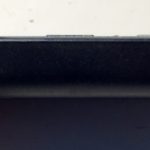
Of course, I didn’t buy it to use it with the stock firmware, so after trying it out, I opened it up to take a look inside. In the process, I managed to tear the translucent plastic that was affixed to the top of the case with adhesive. With the trim removed, it was easy to pry off the top, revealing the single PCB inside.
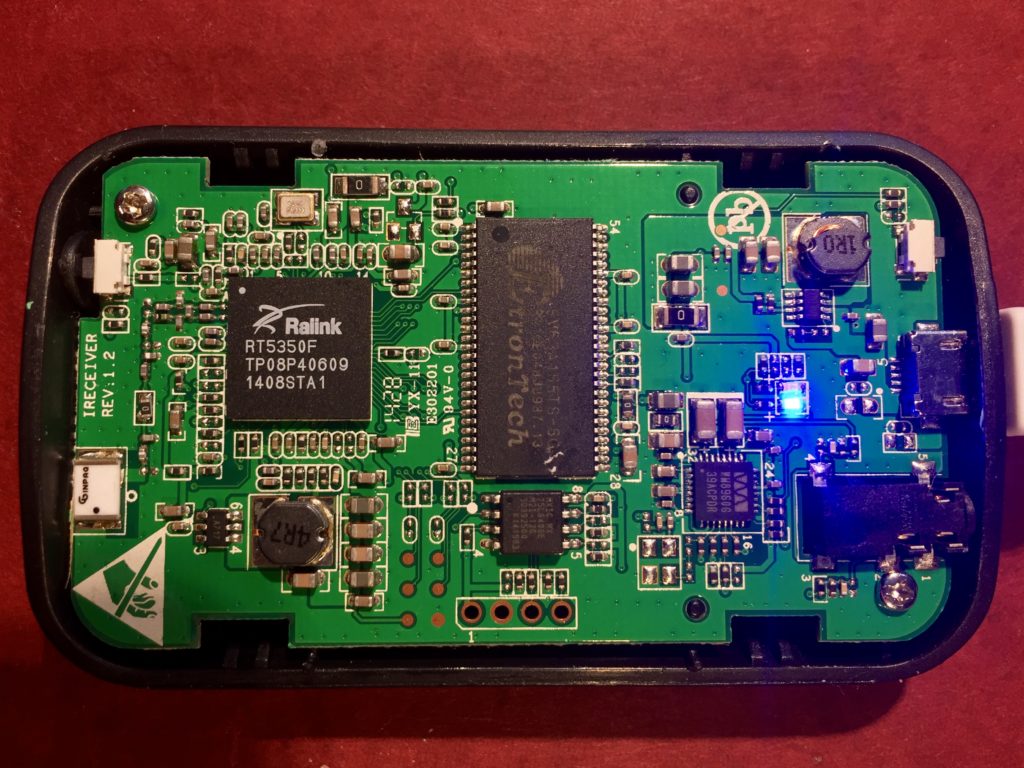
As I expected, it is based on the obsolete but inexpensive and popular Ralink RT5350F WiFi SoC which includes a CPU and 802.11n WiFi.
The other major component is a Wolfson WM8960 CODEC to provide the audio output. This chip debuted in 2006, and includes 24-bit stereo DAC and ADC converters supporting sample rates up to 48Khz, a 40mW headphone driver, and a 1W Class D speaker driver.
Despite being a 24-bit DAC, the specified SnR of 98dBS matches that of the 16-bit TI/Burr Brown PCM2705 DAC used in the original AirportExpress, rather than of a modern, premium 24-bit DAC used in more recent AirportExpress’s. Oh well. Good enough for my purposes. Most of what I’m playing is compressed AAC files derived from 16-bit sources, and, AirPlay only passes 16-bit anyway. Beyond that, the design of the rest of the circuitry matters, and I’m not qualified to analyze it, nor am I equipped or inclined to try and measure it.
Beyond that, I see two inductors on the board (one of which is cracked). My guess is that these are part of some small switch mode power supplies, perhaps one for the digital section, and the other for the analog. There are two small LEDs to indicate device status and two momentary switches, one to reset the device, and the other to trigger WPS. It looks like it uses a single ceramic chip antenna for the WiFi.
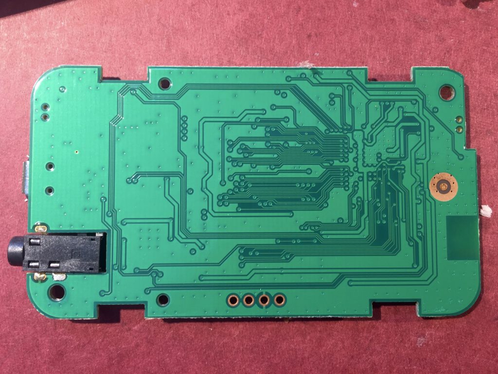
There are a few unused pads for components, eight test points (half seemingly to do with power) and four unused holes for pin headers that I suspect provide a serial console.
That’s really it for the hardware. I’ve already started poking more deeply into the software and investigating the suspected serial console, and I hope to have another post soon documenting what I found.
I’ve passed up a few chances to get a Keithley 2001 7.5-digit multimeter on eBay for ~$500, because while that’s a pretty good deal for a Keithley 2001 in working order, it’s more than I can justify spending on a 7.5 digit multimeter that I want, but don’t need. Somehow though in my twisted psychology, spending $300 on a two-decade older 7.5-digit multimeter with known issues is perfectly acceptable, because I recently did just that.
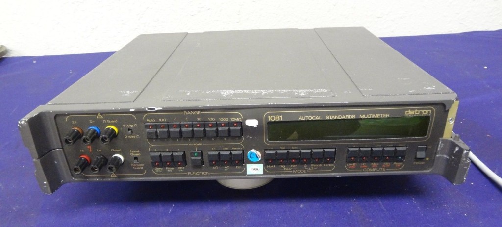
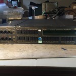
A couple of weeks ago, I was checking eBay on my phone while waiting for an appointment and came across a new llisting for a Datron 1081 Multimeter that caught my eye. It was listed for parts or repair for $300, or best offer.
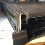
According to the description, it had been damaged in shipping, and gave an error during selftest. From the photos, it looked like the shipping damage was confined to a broken “ear” on the front of the case, and misalignment of the front panel. Definitely interesting…
Some quick googling confirmed that the 1081 was, as I thought, a 7.5-digit capable multimeter with high stability and and the ability to use an external voltage reference. I thought it would be useful for evaluating and calibrating precision voltage references, and 6.5-digit DMMs, like the Keithley 2000 and HP/Agilent/Keysight 34401a. I couldn’t find an operators manual for the 1081, but I hoped the 1071 manual I found was correct that the selftest error was with the AC measurement circuitry. I’m mainly interested in DC, so I wasn’t too concerned.
I reviewed past eBay listings on my phone to confirm that the 1081 typically goes for more than $300, checked my gut, and decided to make an offer of $200.
The seller responded within a few hours that the listing had generated a lot of interest, and counteroffered for $275. At this point, I was back home, with the ability to browse eBay without the limits of a phone. I should have taken advantage of this to investigate past listing a little more thoroughly. If I had I would have realized that some of the higher sales prices weren’t actually sales, they were expired listings that eBay wasn’t filtering properly. I didn’t though, instead I accepted the offer.
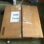
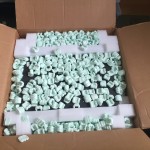
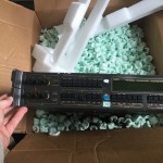
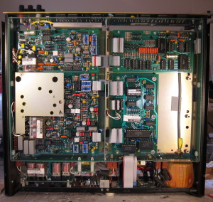
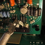
It took a few days for the seller to ship the item, and it was shipped by FedEx Ground, so it took over a week to get to me. It arrived last Friday, packed well in a Cisco router box with reused foam endpieces and packing peanuts for extra protection. It was in the physical condition I expected; the case damage was limited to an extremity, and the main enclosure was sound. I opened it up for inspection and to deal with the misaligned front panel.
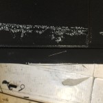
The front panel is a metal plate covered with a big printed plastic sticker. The sticker holds a smoked plastic protective lens over the display. The sticker was loose at a few spots, including the protective lens, which allowed dust and exposure to further weaken the adhesive. I decided to remove it, clean it up, and reattach it.
I heated the panel with a hair dryer to loosen the adhesive, but that didn’t work all that well. I ended up peeling the outer layer and printed layers of the sticker off its backing. Some adhesive remained on on the printed surface of the label, and the backing remained stuck firmly to the metal plate. I used a plastic scraper to remove most of the backing, but getting the rest off required a razor blade, elbow grease, and solvents (“Goo Gone” worked best). I used isopropyl alcohol to clean the remaining adhesive off the back of the printed sheet. Unfortunately I think the process of peeling off the label led to some of the printed brown background along the left side of the lower edge crazing and flaking off. I considered trying to apply a new background of spray paint, but decided the risk of causing further damage wasn’t worthwhile.
Once I got everything cleaned up, I decided to use some non-corrosive silicone adhesive to stick everything back down again. I smeared a thin layer all over the back of the sticker, and around the edge of the smoked lens before lining everything up and sticking it back down, smoothing it out and wiping off any ooze. I weighted the area over the lens and let it cure for a few hours before reattaching it.
Top
Bottom
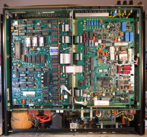
As for the electronics, there sure are a lot of them, and very few of them are electrolytic capacitors – the component most apt to fail on older equipment. I looked everything over very closely.
I was relieved not to spot any physical problems, because while everything is through-hole components, many of them are packed in very closely, and a number of them look like nothing I’ve ever seen before. Repair would be challenging.
My first Glass Capacitors
Actually, there was one problem, but one I expected to find.
The back panel was labeled at manufacture with a battery replacement date of April 1992! Either the battery hadn’t been changed, or whoever did so was too lazy to update the label. Inside I found the truth, the battery had a datecode of 1984, like most of the other components. Fortunately it still had a voltage of 3.7v, but I’ll be changing it soon.
I found a few other interesting things as I looked the device over.
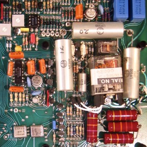
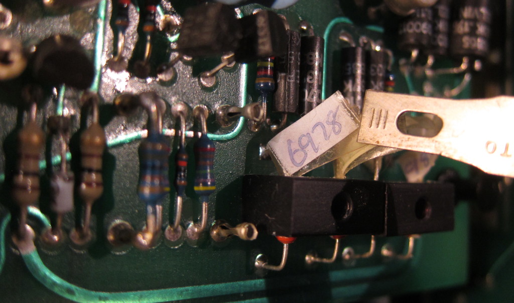
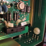
The photos above feature four 1N829a temperature compensated zener diodes. Together, they make up the heart of the voltage reference. They are each numbered with a unique serial number because they were carefully aged for months (or years), then characterized for noise, stability, voltage, and the current at which they have flat temperature sensitivity. My understanding is that the four Zener are connected as two parallel series of two.
I plan to look at these in more detail in a future post, because the unique characteristics of this voltage reference may make it the most notable part of this device. The use of hand-selected temperature compensated Zener was a common practice in a variety of precision instruments at one time, even so, the use of multiple TC Zeners was unusual, as is the stability they obtained. Also by the mid-1980s, when this device was made, use of temperature stabilized burried-Zener voltage references, like the LM199 (introduced in 1976) was commonplace.
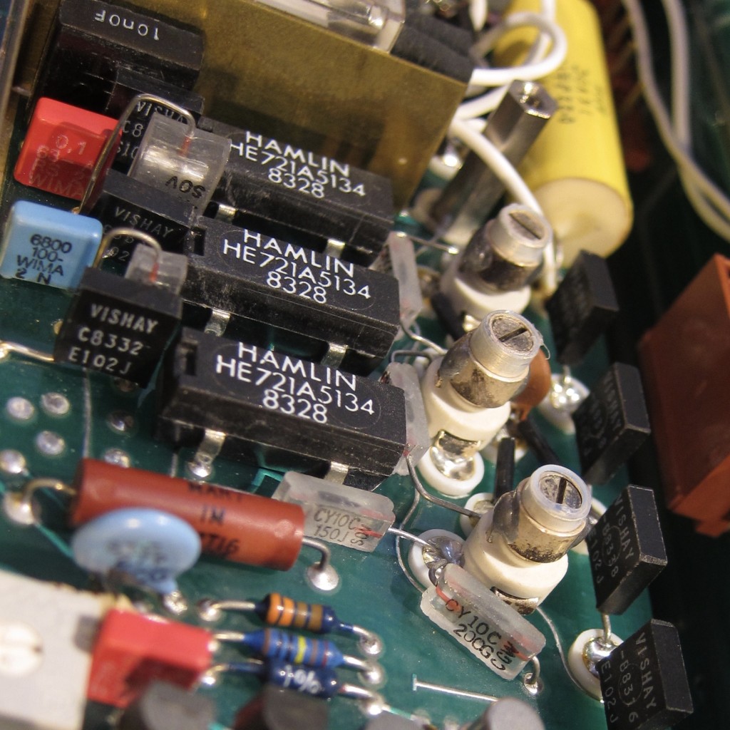
This insulated metal strip running the length of the digital board between a row of I/O bufferes, and the ribbon connectors, also caught my eye.
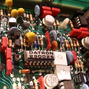
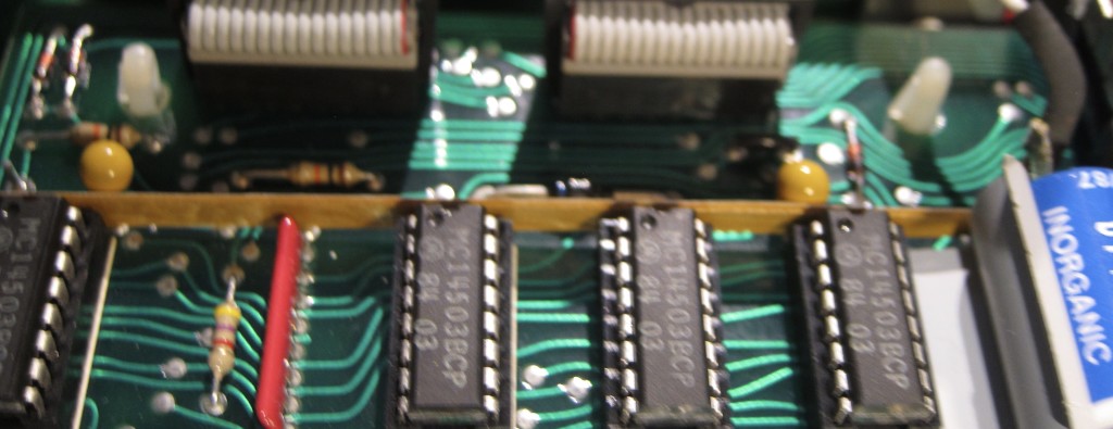
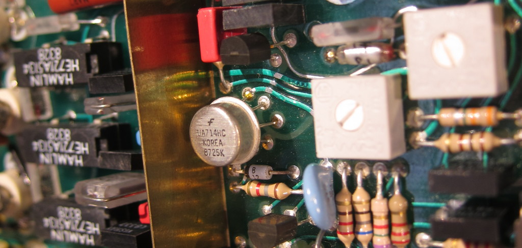
I found evidence of a component level repair on the AC RMS converter board. Most of the components on the AC RMS converter board, and most of the other boards, have date codes no later than mid-1984, but the Fairchild opamp in the hermetically sealed package in the photo above is dated from 1987. The GPIB board seems to date from 1985, and there are some socketed ICs on another board that have 1986 date codes, while other chips on the board are from 1982 or 1983.
Artifacts of repair can also be found on the inside of the case, where some of the melted nubs holding the RF shielding seem to have sheered off and been replaced with some glue.
Functional Tests
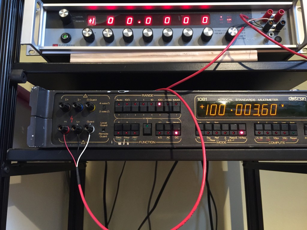
After checking it over and fixing the front panel, I reassembled it, and powered it up. On the EEVBlog forum, “dacman” suggested that self-test error could simply be the result of running the tests with the “guard” switch was set to remote. I could see from the photos on the listing that it was, indeed, set to remote, and it still was when I received it, so I set it to local guard and ran the self tests. Everything passed!
After that, I did spot checks on the 100mv, 1v, 10v and 100v DC ranges using the output from my EDC 521 DC voltage calibrator. The EDC hasn’t been calibrated in years, though from my tests, it is accurate to within the combined 1year tolerances of both it and all my 6.5 digit DMMs. The readings are stable over the short term.
I’ve also done some longer term checks of a 10v signal over a period of days and found that for the most part, the peak-to-peak variation is within the 20-40uV range measured by one of my Keithley 2700s (it is a 6.5-digit meter, but in stats mode it collects and calculates 7.5-digit values) in my Seattle home, near an external wall, without any heating. Sometimes the Datron has reported a wider range than the Keithley, sometimes a narrower range. I’ll need to get logging working over GPIB soon so I can can look more closely at the trends.
Unexpected behavior
In the first few days, of use, I ran into a few instances of unexpected behavior, some of which may have been user error, some of which may have been software bugs, and some of which is as of yet unexplained.
One of the first things to crop up happened while I was checking the 100v range with a 100v output. After the initial readings seemed good, I left it for a while and checked it while I worked. About 15-30 minutes in, I looked over, and it was reporting values of 110v or more, and they were changing quickly. I haven’t been using the EDC much in its 100v range, so I breifly considered the possibility that it was at fault, but a quick look at the Keithley 2700 measuring the same source showed that the voltage was still stable at 100v.
The reading on the Datron was still on the move and soon it was reporting an “Overload.” I tried changing to the 1000v range, but the Overload message remained. I cut the EDCs output and after about 30s, the Datron cleared the overload message and started giving readings again. I applied an input again (I can’t remember if it was 10v or 100v), and it again gave plausible readings. I left it for a while and continued checking it, and after a while, it was again reporting an overload. This time cutting the EDCs output didn’t clear the overload message, and I ended up power cycling it.
Since then, I’ve been focused on the 10v range, and I haven’t seen this behavior again. I have had it with a 100v input for the last 18 hours or so though, and its been solid. I’m beginning to suspect that the problem may have been the result of user error. At some point, I think I’d used a function that “zeros” the meter. I thought this worked like the relative measurement option on my Keithleys, which can give readings relative to any voltage. The Datron 1081’s feature is different. The zero-point is supposed to be set with the inputs shorted, and the value is stored and used until the next time the meter is zeroed. If it is more than a small portion of the full range (1% or so), it will give a overange error. I’m wondering if perhaps the zero-point that I or someone else previously set was near the limit, and perhaps some internal auto-correction ended up pushing things over the limit. This is just a stupid wild ass guess though. All I can be sure of is that since setting the zero point for all the ranges with the input shorted, I haven’t had this happen again.
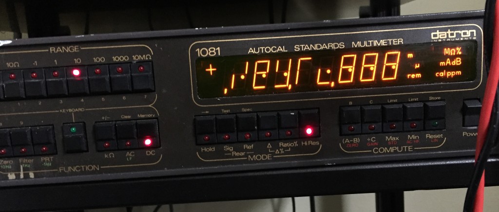
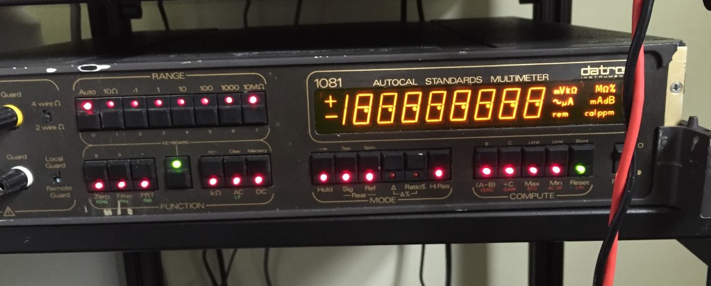
I spotted the next problem after leaving the DMM on overnight. When I checked it the next morning, I suspected that the display had frozen because the last digit didn’t change once. I pushed a button to change the value displayed, and was treated to the above, after a minute or two, it seemed to reset itself and resume operation.
The next morning, after leaving it overnight, I again found it with a frozen display. The first button I hit produced a similar result to the previous day. I tried hitting another button (I don’t remember which) and the rest of the display segments and all the indicator LEDs on the buttons lit up too. This time, it didn’t reset itself, at least not before I got tired of waiting.
I haven’t seen this behavior since, despite leaving the unit on continuously. A few days ago though, I decided to investigate a hunch. I thought that that when I saw this problem behavior previously, I may have left the unit displaying the delta between minimum and maximum values. So, I again left it in that state, and the next morning, the display was again frozen. This suggested that my memory was correct, and that it was infact a software problem. However, the following morning, after again leaving the unit in min-max display overnight, the problem didn’t present itself. So, it seems that I still don’t have it figured out.
What Next
I’m trying to decide where to go from here.
At the very least, I’m going to power it down, open it up again, and take a close look at power supply voltages and ripple.
When I power it up again, I’ll keep an eye out for a recurrence of any of the bad behavior I observed. If so, it will suggest that some of the problems are the result of bad solder joints that act up when the unit is coming to a new thermal equilibrium.
Beyond that, i’ll do some logging over the GPIB interface to get a better sense of stability and tempco. I also need to investigate the resistance and ACV functions.
After that, I’ll have to consider whether to get it calibrated, or figure out a way to calibrate it myself. I’d also like to investigate its ability to use an external voltage reference to provide high-precision comparisons between different voltage standards. Doing so will require either figuring out a source of the (likely expensive) low-thermal-EMF rear panel connectors, or replacing them with similar performance and lower cost.
I’m also still looking for a Datron 1081/1082 Users Handbook (the 1082 is basically a 1081 with all the options). The Datron 1051/1061/1071 users handbook has been useful, because for the most part, they operate very similarly to the 1081, but there are some important differences with the digital filter, and some of the other aspects.