Ravpower USB PD Powerbank Teardown

A couple of years ago I bought a Ravpower 30W USB PD powerbank with one USB Type-C port, and two regular 5v USB ports.

It was a little quirky. Sometimes it would start charging itself from the laptop until I held the button down for 5s. At some point the behavior started getting worse, to the point that last summer I left a poor review. The seller contacted me quickly, and I had a replacement within a week. The replacement fixed the problem.

That left me with the defective unit. Today, I decided to take it apart and see what’s inside.

The highlights are:

  • A sturdy ABS case
  • 8x LG F1L 18650 cells
  • One PCB
    • Sonix SN8F57 8-bit 8051-based microcontroller
    • Cyprus CYPD2122 USB PD port controller
    • Southchip SC8802 buck-boost charge & discharge controller
      • Regulation of voltage and current for lithium ion battery charging for 1s-6s battery packs (4.2-25.2v)
      • Charging current to 10A!
      • Input voltage from 2.7-30v
      • Output to load from 2-30v & 60W

The pack sells for ~$75. To put things in perspective, you can buy eight FL1 cells for $4.41/each, which works out to about $35. That price drops to $3.56 each through a grey-market seller if you buy a thousand at a time. Ravpower is almost certainly paying less than that.

You can see more in the YouTube video I shot of the process:

Datasheets:

What IC does the MH KC24 USB QC2/3 Buck Module Use?

I want to know what IC is used on this MH-KC24 USB power module I received.

This module, like the MH-CD42 module I looked at recently, has a single IC with unhelpful markings. Since the IC on that board appears to be from Injoinic Technology, I thought the IC on this module might share the same origin.

I reviewed the product offerings on their English language site and thought the ICs for car chargers looked the most promising. Based on the summary specifications, the IP6505 fills the bill. This IP6505-based module certainly carries the same supporting components, and the IC shares the same footprint.

The IC combines an efficient synchronous buck converter and logic for negotiating power delivery using a variety of USB charging protocols. My primary interest is in Apple 2.4A/12W charging, but it also supports Qualcomm’s QC2 & QC3 protocols, which is popular among android smartphones using Qualcomm’s SoCs.

I see that their IP6518 IC, which supports 45W USB PD charging is available on inexpensive modules, too.

Balight 21W Folding Solar Panel USB Charger Partial Teardown

I picked up a 21W, 3-panel Balight folding solar panel-based USB charger from Amazon for ~$36 a couple of weeks back. It uses high-efficiency SunPower Maxeon cells much like similar 20-21W panels from AukeyAnker and dozens of obscure brands. All of them have the same basic construction. They are all made from nylon ballistic cloth. Each fold has a panel made from two SunPower cells encapsulated in a flexible waterpoof sheet. The panels provide power via two 5v USB ports, which presumably have some sort of voltage regulator.

I wanted to know more about how the chargers worked. In particular, I wanted to know if they were wired in series, or parallel because I wondered if it was worth trying to tap into the raw output, before the USB regulator to reduce power conversion and resistive losses for some applications.

I thought I’d be able to get the information I needed by finding someone documenting a teardown of their own panel on YouTube or a blog post. Despite the dozens of variants from dozens of brands and a handful of manufactures though, I didn’t find what I was looking for.

So, I decided to dig up a seam ripper and open my panel far enough to get a look at the wiring, and tap in to it upstream of the voltage regulator.

The panels appear to be wired together with some sort of woven wire conductor. I had some hope that all the cells would be wired in series, to give a nominal panel voltage of 18v. Based on what I could see, and measuring the voltage before the regulator in full sun, it looks like each panel is wired in series, for 6v nominal voltage, and then the panels are wired together in parallel. I was disappointed at first, but this arrangement makes sense in upon further thought.

Using a 2s3p configuration means that the input voltage into the switching regulator should be pretty close to the 5v (actually, 5.2v with enough sun and a light enough load) output of the USB power regulator, which will typically have higher conversion efficiency than 12 or 18 volts. It also means that the manufacturers can stock one converter for everything from a 7W single-panel charger, up to a 28w 4 panel charger without the converter having to support a wide range of input voltages. Perhaps most importantly, it means that partial shading of one panel shouldn’t have a disproportionate impact on the power output of the entire array.

The only downside is that resistive losses in the cabling will be higher with lower voltage and higher current, but that the interconnects aren’t more than a foot or so, the resistive losses shouldn’t be too high.

As for the converter itself, I may look at it more closely and add some more details, but, a few initial observations:

  • The PCB design has extensive ground planes on top and bottom, tied together with vias.
  • Both outputs are served from a single buck-converter (step-down) power supply based on a Techcode TD1583, which is a 380 KHz fixed frequency monolithic step down switch mode regulator with a built in internal Power MOSFET.
  • It looks like only port 1, at the top right in my photo, has the data lines connected, which suggests that it is the only one with fast-charge coding.
  • IC U2 looks like it has its markings sanded off. I notice though that one of its pins is connected to the enable pin on the TD1583, leading me to think that it is responsible for cycling the output to make sure devices draw as much power as possible when the panel voltage rises again after clouds or an object reducing the light falling on the array pass. I don’t know if it is a MCU, some sort of timer, or comparator, or what, though.

There you go. I can’t be sure that other folding solar arrays like this one are wired in the same way, but if they only support a 5v output, I suspect they will be. I hope this proves useful to someone besides me.

Mac OS X Kernel Panics with RTL-SDR/RTL2832U and Analog Discovery, and a Fix

Earlier this week I fired up WaveForms in order to do some spectrum analysis of power supply rails hooked up to a Class D amplifier board using my Analog Discovery. Before I got the Analog Discovery plugged in though, my computer froze, the screen went dark, and then a kernel panic error displayed.

This was new, I’ve never had a problem before, whether or not the device was hooked up before firing up the software. I tried again, this time making sure the Analog Discovery was plugged in before launching Waveforms. Another kernel panic. I tried again, this time plugging it directly into my laptop, rather than the USB3 hub I use for convenience. Another kernel panic. I muttered and cursed and speculated that the cause was the OS X 10.11.6 update I’d recently installed, and ended up using a Windows machine for the task instead.

A few days later, I received a cheap RTL2832 USB DVB receiver I’d purchased in order to (finally) experiment with Software Defined Radio (SDR) using RTL-SDR software. My first explorations were tacked from base camps on my patio and bed. Everything worked without issue. The third time though, I was at my desk, and as soon as I launched CubicSDR my computer froze, went black, and then complained of a kernel panic.

I was peeved. I thought, perhaps that my hub was an issue, so I plugged the RTL2832 in directly. It worked. I tried a different hub. It worked again. I tried something else, it crashed.

Eventually, I figured out that the problem only occurs with a USB3 to Gigabit Ethernet adapter connected (with or without a hub involved). The adapter in question is based on the RTL8153 chip, which is used in USB3 to GigE adapters sold under many different names.

This chip is complaint with standard USB Ethernet protocols, and works with generic drivers provided by Apple in OS X 10.11 (El Capitan), and perhaps earlier versions. I’d installed the Realtek provided driver in order to take advantage of some features of the chip which might improve performance and power consumption, but not to a significant degree.

By removing the Realtek RTL8153 driver using a script provided in the installer package, I was able to revert to using the generic apple USB Ethernet driver. Now, I can use my Analog Discovery with Waveforms, my RTL-SDR with CubicSDR, and my USB3 Ethernet adapter at the same time without Kernel panics.

KMASHI 10,000 mAh USB Power Bank / Backup Charger Teardown

I decided to buy a USB “power bank” or backup external battery to keep in my backpack to recharge my phone or iPad when I am away from the house.

I looked at lots of options over the course of a few months before I pulled the trigger. It was hard to make the decision because their seemed to be a big variance in capacity, price, and charging rates. What finally tipped me over the edge was finding a 10,000 mAh unit that could charge external devices at 2A and recharge at 2A for $17.99. Actually, the numbers associated with the model I purchased, (KMASHI 10,000 mAh) USB specs aren’t that unusual, but often times, the devices fall short of their claimed capacity. In this case though, there was a review by someone who’d done some testing and found that it pretty much hit the mark (though it did seem to fall short in the rate it charged USB devices).

When I received the product, I was a little disappointed. It worked as promised, and seemed solidly made, but It was bigger and heavier than I’d expected, and so I decided to crack it open to find out why.

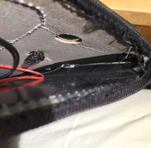
It took some effort to get it open. I thought it might be glued shut, but with a little effort, I was able to persuade some of the latching tabs that held the case together to slip free by jamming something into a seam and working it around.

IMG_5700
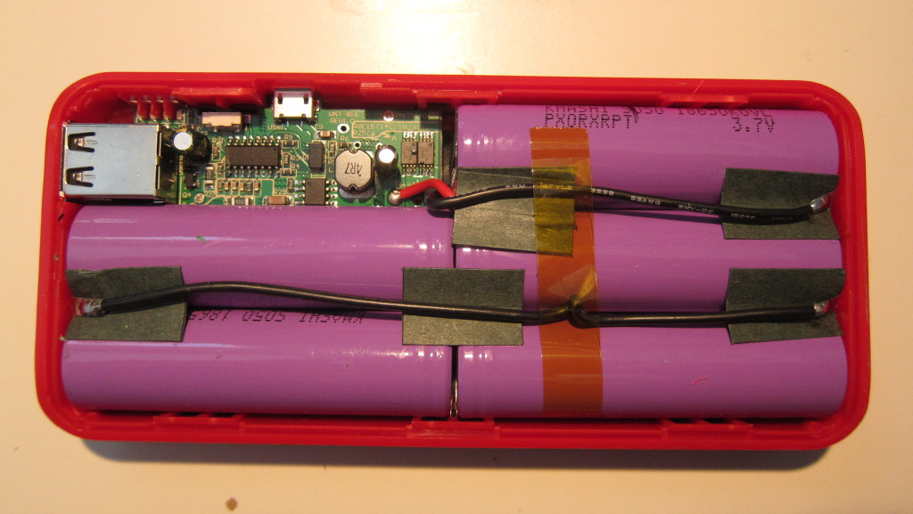
This is what I found inside. As you’d expect, a good portion of the volume is taken up by the batteries, five cylindrical 18650-sized lithium ion cells. This is the reason for the size and weight of the device. First off, the cylindrical cells don’t pack together as tightly as flat-pack pouch cells found in most phones, tablets, and higher end USB battery packs. Second, their steel walled container weighs more than the plastic membrane used on flat pouch cells.

The bigger issue though is that there are five of them, which means that they must each have a capacity of only 2,000 mAh. That’s not much. 18650 cells (which stands for 18mm diameter, 65.mm length) are widely used for laptops, battery powered tools, and even Tesla automobiles. I pulled some 18650 cells out of ~5 year old laptop battery packs that are rated for 2,600 mAh and still deliver ~2,550 mAh. More recent laptops use cells with 3,000, 3,200, or perhaps even 3,400 mAh capacity, so it would be possible to build a power bank of equivalent capacity with four, or as few as three cells, with a corresponding reduction of weight and size.

On the other hand, those larger capacity cells from Panasonic, Samsung, Sony, and others, retail for $6-8/cell, and 2,600 mAh cells go for ~$3-3.50. I am sure these cells were much much cheaper.

IMG_5701


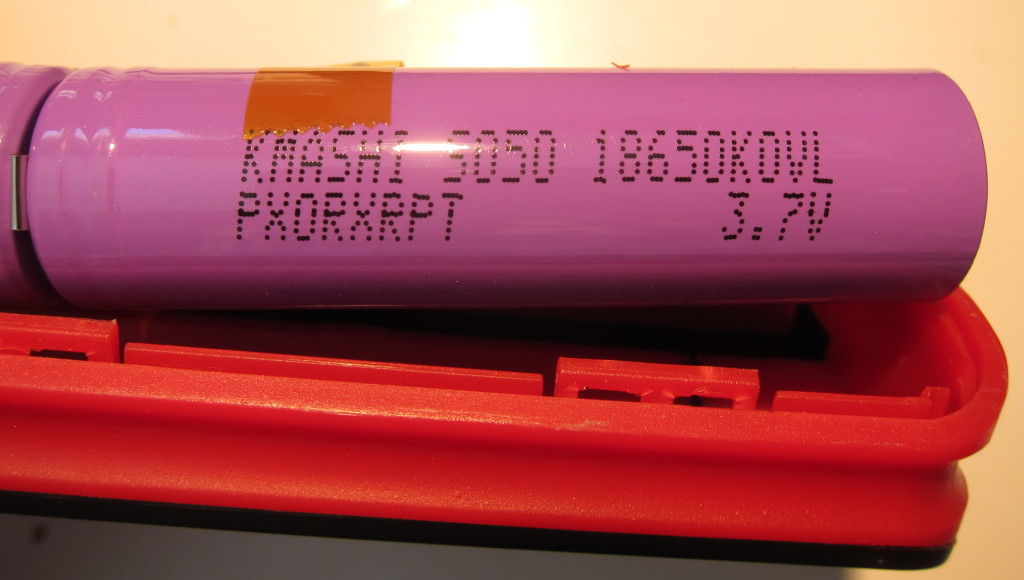
The cell wrappers are labeled “KMASHI SO50 18650KOVL PXORXRPT 3.7V,” This doesn’t give much of a clue as to the true origin of these cells. KMASHI doesn’t appear to be an actual battery manufacturer, that comes up in other contexts. 3.7V is the typical voltage for lithium ion cells, and 18650 is a common form factor, but searches for any of the terms on the label doesn’t produce useful results. I could cut the wrap off and see if there are any clues printed on the metal, but then I’d have to rewrap the cell, which would be a pain since they are all welded together.

So, who knows what kind of cells these are, they might even be reused used cells, for all I know.

IMG_5702

This photo shows that the cells have been spot welded together in a parallel configuration, which is commonplace in multi-cell USB battery packs. I suspect the parallel approach is typically used for a few reasons. First, it should be more tolerant of lower quality cells than the series-configuration. Second, it should pose less of a risk of frying the USB device if the voltage regulation circuit is funky. Finally, it makes it easier to charge the pack off of a USB power adapter.

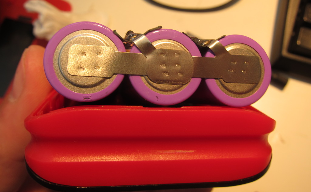
Looking at the end of these cells gives another hint that these may be reused cells. From my experience, raised bottoms are unusual on 18650 batteries, and others have reported that they are often used to hide the evidence of old welds on cells that have been pulled out of assembled battery packs.

If they are reused cells, that causes me some concern. If they are good quality cells from battery packs that just sat on the shelf (aka New Old Stock), then it would be a non-issue as I have obtained cells that way myself. If they’ve actually been used, or if they are from very old packs though, thats a problem, as they could fail prematurely, and failing lithium ion batteries can be dangerous.

IMG_5699


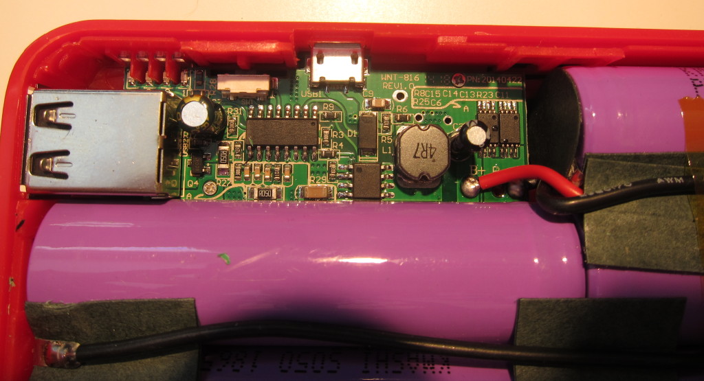
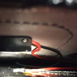
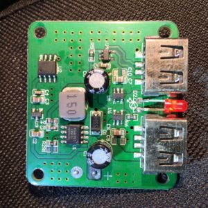
For completeness, I give you the printed circuit board, which is labeled as “WNT-816 Rev 1.0” and “PN:20140422” on the top. I can’t say much about the components. The two largest chips appear to have been sanded to obscure their origins. There are two other chips that have their markings which read “FS8205A,” near as I can tell, they are used for managing the discharge of lithium-ion batteries.That, and the inductor is solid-core, unlike the many hollow-core inductors I’ve seen on the powerbank PCBs they sell on Fasttech.

IMG_5705

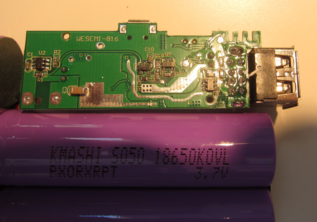
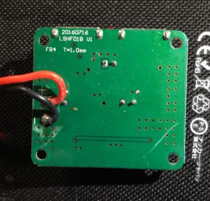
On the bottom, it is labeled “wesemi-816.”

I reassembled it and I’ve used it since taking it apart. It works pretty much as expected. I’ll post an update in a few weeks once I get some stuff I ordered for testing USB power sources.