A helpful list of Mac compatible instrumentation.
Mac Compatible Instruments & Test Equipment
Link
Reply
A helpful list of Mac compatible instrumentation.
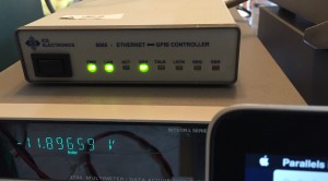
I got a pretty good deal on eBay for an ICS 8065 Ethernet GPIB Controller. When it arrived, I reset the network configuration by holding down the reset button on the back panel while turning on the unit and waiting 10 seconds. This set the unit to its factory default IP address of 192.168.0.254, so I could connect to it from a web browser on my laptop.
Once in, I found that the installed firmware was years out of date, and set out to update it. Unfortunately, the firmware can’t be updated from a web interface. It is necessary to use a Windows utility. I’m not really a Windows user, though I have a Windows machine in the house. Using it would require more fussing around with network connections than on my laptop, which I plugged directly into the 8065 while using WiFi to communicate with the rest of my network, and browse the web.
I didn’t even consider running the software in WINE, opting instead to use a 64-bit Windows 7 virtual machine on my laptop. Unfortunately, when I tried to run the updater program in the firmware update ZIP file I downloaded from the ICS Website I was met with an error that comdlg32.ocx wasn’t registered.
After a bit of googling, I found a solution, which I’m sharing here for anyone else who runs into this. Comdlg32.ocx is somewhat dated software. I don’t know if it was part of earlier versions of Windows, or whether it was the responsibility of applications to distribute it as part of their installer package. What I do know is that the ICS Firmware updater doesn’t have a Windows Installer, that comdlg32.ocx wasn’t included the zip file with the firmware, that it wasn’t anywhere on my system, and that I haven’t installed many other applications.
From there:
Once I did this, I could double click and run the “M805_update.exe” program without error and update the firmware.
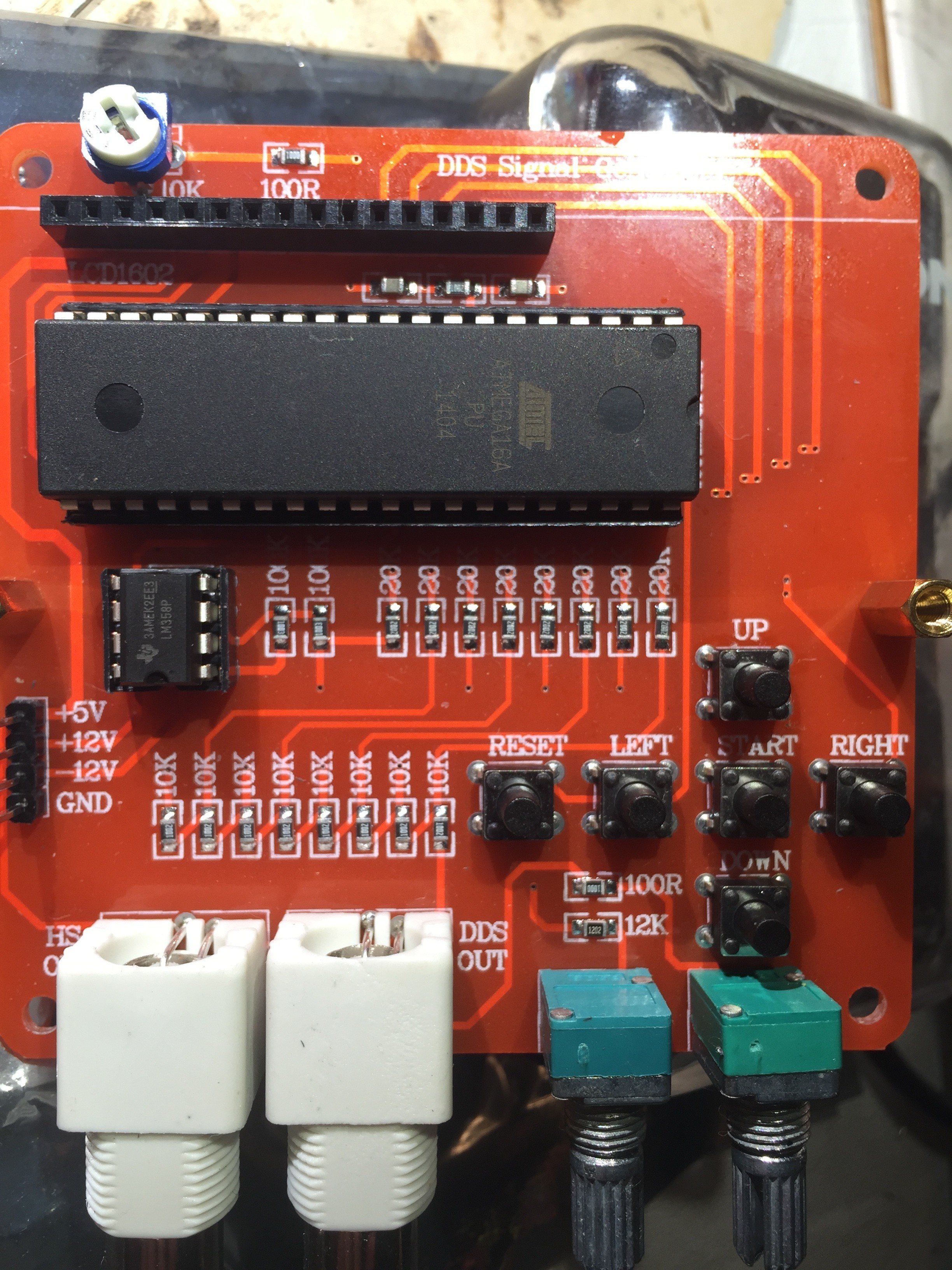
Months ago, I bought a $15 AVR-based DDS signal generator kit from eBay. I didn’t have high expectations, but I thought it would give me a capability I didn’t currently have, and give me the chance to practice soldering.
It was immediately clear upon opening the package that it was at least half a failure, because it was fully assembled. For this, I got a partial refund, making it a ~$10 fully-assembled DDS signal generator.
It sat a few months while I acquired, refurbished, diagnosed, and ultimately repaired a used Power Designs TP340A three output bench power supply that I could use to provide the +15, -15 and +5V needed to power it.
Once I had it powered up and hooked to the scope, it took me 5-10 minutes to figure out how the thing worked. The digital controls are a little odd, but easy to figure out. The outputs and analog controls are a little fussier. Ultimately though, I figured out that the leftmost BNC is for a high-speed square-wave output. The right BNC is for the synthesized DSS output, the leftmost potentiometer is for amplitude, the right for DC offset.
It didn’t take too much longer to see how badly this thing sucks. At first glance the 2 KHz sine wave doesn’t look too bad
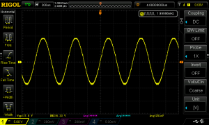 If you look closely though, you see some consistent glitches. This thing generates an analog value by switching resistors using the AVRs GPIO pins. My guess is that this glitch is caused by one or more out of tolerance resistors.

Looking even more closely, you can start to see high-frequency noise. In his Youtube review (embedded below), Electron Update notes that this noise has a frequency of 1MHz and believes that this is probably noise from the digital section.

The 2KHz square wave isn’t too great. The rise and fall times are rather significant relative to the on/off times.

At 20KHz, the square wave is a sloppy triangle. Note too that the peak-to-peak amplitude is only 6.56v vs the 18.2 it delivers at 2Khz.

The “high speed” 20KHz sine isn’t very good either. The waveform is nearly identical to that of the 20KHz square wave, and like the square wave, the peak-to-peak voltage of ~6.6v is a fraction of the 17.8v excursion at 2KHz.
Of course, 20KHz isn’t really high-speed at all. Its at the top end of the human auditory range. The device actually supports up to ~65KHz. It doesn’t get better. The truth is, the waveforms go to hell before 10KHz.
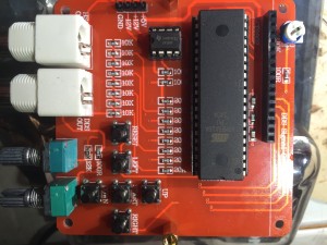
My device seems to be based on the AVR DDS signal generator V2.0 software and hardware from 2008, with minor revisions to the hardware for manufacturability.
Electron Update did a review/analysis of a similar device based on the same design on his youtube channel.
The design has some fundamental limitations, thought it isn’t clear if some of my problems are specific to my unit.
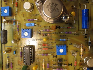
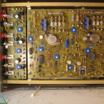
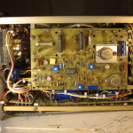
An update on the Power Designs TP340A bench power supply I’ve been restoring and repairing. I started by replacing a bad Sprague electrolytic capacitor. While I was at it, I decided to replace all the big electrolytic caps. That didn’t go so well, because I put two of them in backwards and caused them to vent. After replacing the vented caps, I noticed that the supply wasn’t behaving quite right, and found that some key voltages were out of spec. After some trial and error, I figured out which components to replace to get everything in spec.
I was pretty pleased with myself, but the next morning I realized that I’d been too hasty to write off some drift I encountered while calibrating Source B. I started load testing Source A & B, both separately, and in tracking mode while watching the output on a multimeter, and my oscilloscope in roll-mode:
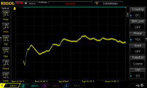
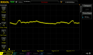
It didn’t take long before the voltage of the output on Soure B started a random drunken walk over the range of a 0.5v or more. After a while, it stabilized again and I left it to run a few hours without incident.
Before turning things off, I started fiddling around, connecting and disconnecting things, varying the current and voltage, trying to provoke another excursion and before long, it did it again. I really wasn’t sure what was going on, and figured I’d need to consult the schematics and start a long process of trying to figure things out.
Lucky for me, over on the Eevblog forum, user nanofrog, who’d helped me pick out replacement capacitors, checked in on my progress and I shared what I just described above. He replied suggesting I look for thermal-related issues, like a bad solder joint. That made sense! I didn’t have any obvious problems when the unit was running, just when it was heating up and cooling down.
I spent a good chunk of my 4th of July indoors, in a warm, dimly lit room, abusing the PCB of my power supply with alternating blasts of hot air from a hair dryer and cold spray from an inverted can of electronics duster while measuring things with my scope and DMM. I also loosened mounting screws so I could flex the PCB. I wasn’t getting the dramatic results I was hoping for, but eventually, with enough persistence, I was able to get bad behavior by focusing my attention on the lower part of the board near C211. From the schematics, I could see that C111 had a role in damping feedback going to the main voltage regulating op-amp. I inspected the PCB closely looking for a bad solder join on this capacitor, or any of the components in circuit with it.
After a good hour spent squinting and angling to get a better look I hadn’t found an obvious problem, but I saw a few solder joints that I was suspicious of. So, I heated up my soldering iron, daubed on some RMA flux and made sure I had some leaded solder handy and got to work touching-up the questionable joints.
Then I started testing it again. I repeated the cycle of heating and cooling multiple times without obvious problems. This morning I got up and did it some more, then left it running for a couple hours before calibrating it again.
This time, I didn’t run into any drift during calibration, but having declared victory prematurely once before, I wasn’t ready to call the project done. I needed more convincing.
Earlier in the troubleshooting process, I had noticed some subtler behavior when the PSU thermal equilibrium. All though Souce B’s voltage was stable from second to second and minute to minute under a steady current, it had poor load regulation, with changes of ~30mv or more when between 0 & 1A of current. Moverover, if I used the statistics function on my Keithley 2700 multimeter to take 1000 readings of the voltage while the unit was under a constant load, I found that the Standard Deviation in reads was 10x higher for Source B compared to Source A.
First, I checked load regulation of both Source A & B between 0 and 1A at ~10V. Both had a total swing of ~3-4mv. According to specs, it should be ~2mV. My measured values are worse, but not dramatically so, and also pretty similar between channels, suggesting to me that I’d managed to fix the major instability issue.
Next thing I did was take 1024 readings for each source with a constant load of ~1A, again at 10V. Both channels had a standard deviation of ~25-30uV, whereas previously, channel B would have been 10x. More evidence that I’ve indeed solved the major instability problem.
I haven’t checked transient response or ripple, or thermal stability or long-term stability, but for the things I have checked, this PSU is very close to its original specs. Its also good enough for my purposes right now, so I’m going to call this project done and move on.
Previously I wrote about my clumsy efforts to refurbish a TP340A triple-output bench power supply I bought on eBay. The seller listed it as used, implying it was fully functional, but I was skeptical and opened it up to check it over. I found a bad electrolytic capacitor, and decided to replace all of them. In retrospect, I should have asked the seller for a partial refund, but I didn’t.
After I finished replacing all the electrolytic caps, things didn’t seem quite right. Source A seemed fine, but when Source B was set to track Source A, its voltage didn’t rise until Source A reached ~8V, at which point Source B jumped from ~0v to ~8v. It then tracked with Source A until reaching ~16V, and then started dropping off again.
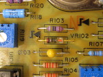
So I started working through the troubleshooting steps in the manual and checked the regulated B+ voltages measured on capacitors C104 (Source A) C204 (Source B), and C304 (Source C) are stable and fall within 12.4v DC and 13.2v DC.
B+ Voltage
Source A: 12.61v
Source B: 12.26v
Source C: 12.04v
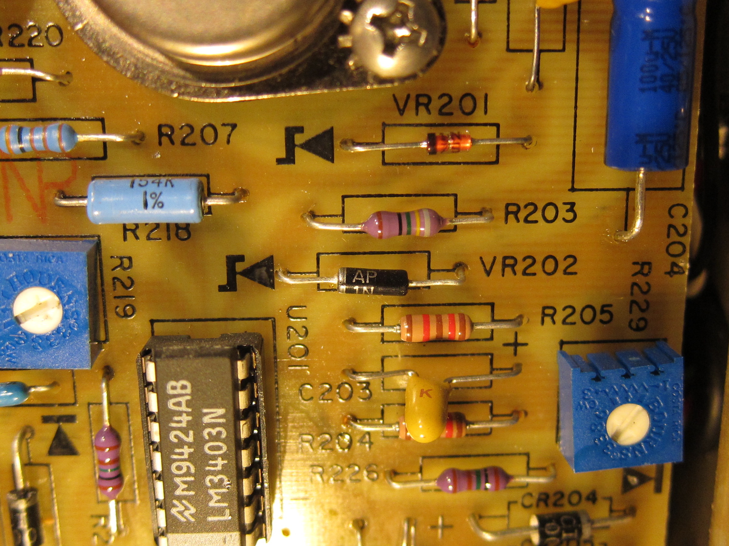
Clearly something wasn’t right, the values for Source B & C were out of spec. I continued by checked the voltages across the zener diodes VR103, VR203, and VR302 (nope, VR302 is not a typo).
VR103: 5.682v
VR203: 1.728v
VR302: 5.688v
Better here, in that two of the values are in spec (5-5.8v), but the value for Source B is WAY out of spec. Next steps, according to the manual, are to check for defective components, in order, capacitors C201-204, rectifier diode CR201, transistor Q201, VR201, VR202, VR203, and U101.
I’d already replaced C201 and C204, so I skipped that. I didn’t have great tools for checking components in place, so rather than starting to remove and test them, I first measured other components.
Main Source Reference Voltage
VR102: 6.31
VR202: 6.126
VR303: 6.010
These should fall between 6.26 and 6.52v. Only Source A is within spec.
VR101 5.629
VR201 5.639
VR301 5.619
These all check-out, falling in the range of 5-5.8v as they should.
I lifted a leg on C202 and C102 so I could compare the values. I measured them with my AVRTransistortester with some test clips on leads.
C102: 1093nF, 6.9Ω ESR
C202: 1085nF, 1.0Ω ESR
Different, but different enough to be responsible for the other symptoms? I didn’t have any idea, soo, I ordered some 1µF, 50v Kemet Tantalum capacitors and replaced C202 and C203 with them. The result? No obvious change.
Next I wandered even further off the troubleshooting guide. I pulled VR202 to test it. As it turns out, I tested it to failure. No problem, right? Zener diodes are cheap and plentiful. I thought I probably had a suitable replacement in a semiconductor assortment I bought a few months back. Nope, nothing for that voltage. Time for another cycle of selecting a replacement, ordering it, and waiting for it to arrive.
Well, it turns out, selecting and ordering a replacement was a little harder than I expected. According the the manual, VR102, VR202 and VR203 are 1N825 zener diodes in grades G through K. Type 1N825 zener diodes aren’t run of the mill parts, they are part of a family of temperature compensated 6.2v zener diodes.
The family is made by creating a zener and a regular diode on the same piece of silicon in opposite orientations. In operation the negative temperature coefficient of the forward biased diode helps balance the positive temperature coefficient of the reverse-biased zener. The diodes are then burned in, characterized, and selected for appropriate temperature compensation. The 1N825 has a maximum temperature coefficient over its operating range of 0.002%/C. The family has the following temperature coefficients:
1N821: 0.01%/C
1N823: 0.005%/C
1N825: 0.002%/C
1N827: 0.001%/C
1N829: 0.0005%/C
There are also parts with the A suffix apply, which means they have maximum dynamic impedance of 10 Ohms, rather than 15 for the other grade. These were state of the art when they were introduced in the 60s, and have had a long run (my power supply was manufactured in the mid 1990s), but they’ve been superseded by other voltage reference designs.
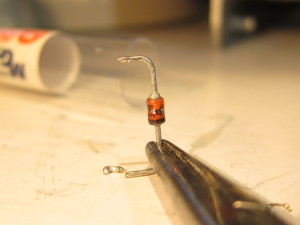
In my initial searching, I only found references to 1N825A parts, not 1N825G, 1N825H, 1N825I, 1N825J or 1N825K, as described in the Power Designs part list in the manual. I figured they were probably proprietary Power Designs designations, but I decided to dig around more just in case. To help in that effort, I looked closely at the actual markings on the diodes. It didn’t help much.
AP
1N
825
The only new information was the “AP,” probably a manufacturer code, and the absence of the A suffix. My best guess is that the manufacturer code might be for American Power Devices, which manufactured 1N825 diodes.
In my wanderings, II found someone who claimed, based on experience, that newer 1N825 zeners had more problems with noise. At least, I thought I found someone who claimed that. I can’t find the source now. In any case, based on that, perhaps imagined, information, I decided to go looking for new-old-stock parts, rather than new parts from Mouser or DigiKey. I found someone on ebay selling Motorola-made military-spec 1N827 parts on ebay in lots of 4 for about $10 with shipping. Given my poor track record of ruining parts, I decided to buy 8.
With the new diode in place, I was back to where I started. Time to do the obvious thing and check VR203, the zener diode that was running at 1.7v, rather than the ~5.6 specified. The part number for this in the manual is 3EZ5.6D5. Without much effort, I found this number in an old Motorola diode catalog. Motorola’s spec is Glass, 5.6v, 134mA test, 500mW, 480mA max, and they cross reference it with the industry standard 1N5014.
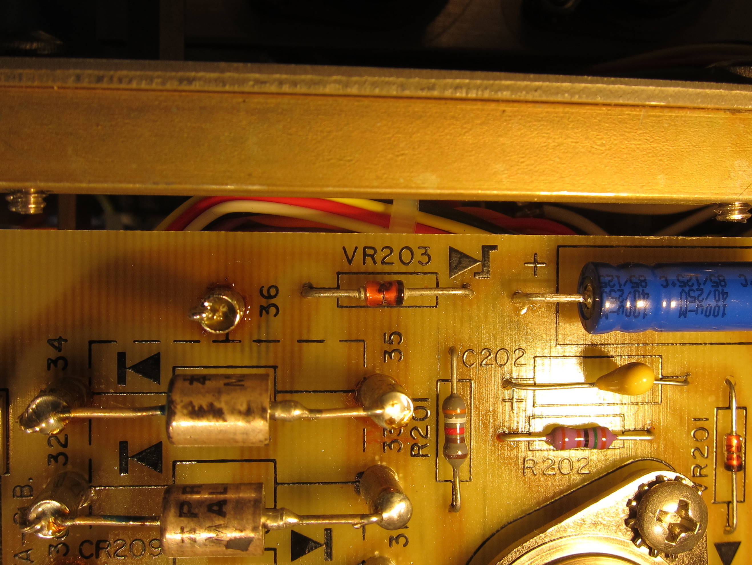
Time to check the actual part. I desoldered it to check it and test it. This time I avoided ruining the thing, helped, perhaps in part, by the fact that it was clearly already ruined. Time to figure out a suitable replacement.
I checked the diode for markings. My eyes have gone downhill quickly in the last couple of years, so I deployed some optical assistance to determine that the diode was marked with the following.
1N
47
34
A
There was also a logo, which looked a lot like an older National Semiconductor logo. That made it a 1N4734A zener diode, not a 3EZ5.6D5 or a 1N5014. The 1N4734A is also 5.6v zener like the 3EZ5.6D5, but the test current is only 45mA. I ordered some NXP (successor to NatSemi) 1N4734A zener diodes from Mouser and, again, waited.
A few days later, the package arrived. I soldered the replacement zener into place, and plugged the PSU in, powered it up, and checked the voltages again. Success! Source B’s voltages were now in spec! On to Source C!
With source C, rather than checking caps and whatnot, I went right to the component that was out of spec, VR303, which had a voltage drop of 6v, rather than the specified 6.2-6.5v. First thing I had to do was double check the schematic to make sure I was looking at the right component. Most of the components in this section of all three sources have similar labels to the analogous parts in the other sources (ie C101, C102, C103) but for some reason, they broke this convention with the main voltage reference for Source C, VR303, rather than VR302.
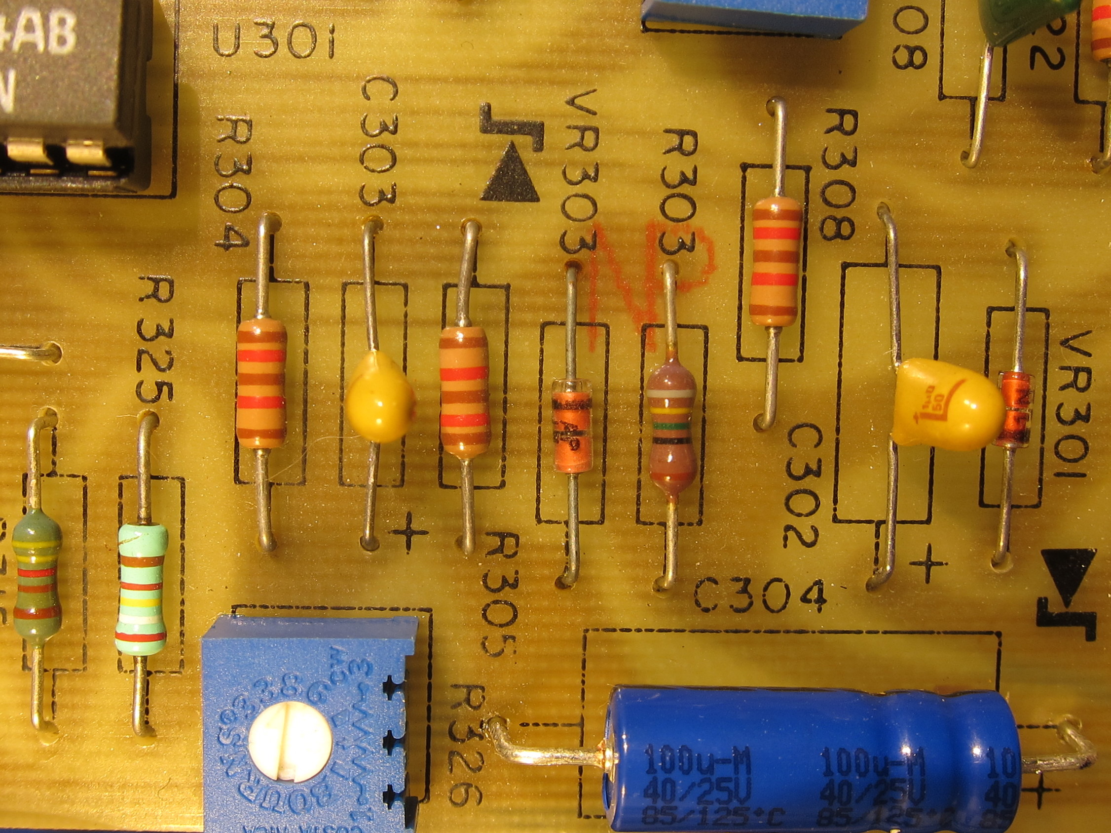
Apparently I’m not the only one who got confused. I had to check I was looking at the right component, again, because while this was supposed to be a 1N825 like the others, it didn’t have the same thin black package and slender leads. In fact, it looked a lot like the 1N4734As I’d just dealt with. Once I pulled it out and got it under a magnifying glass, I saw that it was, indeed, a 1N4734A. I wonder who made the mistake? Most likely it was a botched repair.
Installed one of the extra 1N827s to fix the mistake, and decided to replace V102 as well, so all three channels would have similar parts of similar vintage and tempco for their main voltage reference.
This time, when I powered it up, all the voltages were in spec. I did a little load testing and things seemed to check out. No more strange behavior with Source B lagging Source A in tracking mode, and it was able to deliver full voltage and full current on all channels. I moved on to calibrating the meters, adjusting the maximum voltage, and correcting the tracking offset.
I felt giddy, I’d fixed it! I was done, or so I thought. The next morning though, the sun woke me up early. As I was trying to fall back asleep I thought of something that had happened while I was adjusting the PSU the night before. I wasn’t done.