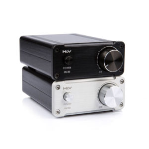
I’m asking, but I think I already know the answer: No, no one knows anything about the SMSL HV-50 audio amplifier, or if they do, they aren’t talking (not in english, anyway). I found a recent reddit thread asking about it, but no one knew much, and I haven’t found much else.
The TDA7492 chip is used in a lot of compact, inexpensive audio amps made by various Chinese manufacturers and sold under various names on Amazon, Ebay, AliExpress, etc.
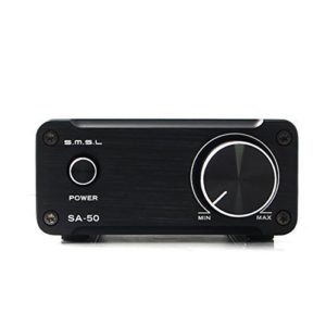
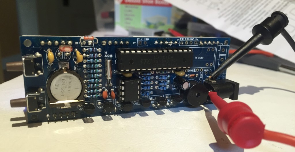
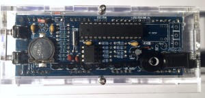
SMSL SA-50
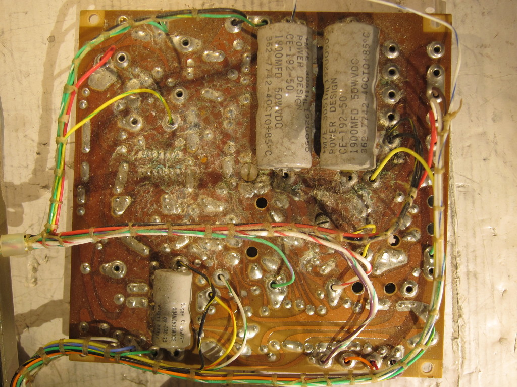
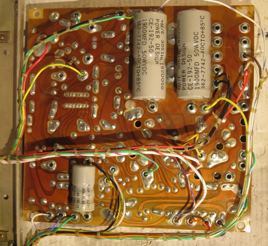
It is also used in the older, almost identically specced 50 Watt/channel SMSL SA-50 amplifier, pictured above. The chip and specs aren’t the only thing the two have in common. As you can see, the case is the same. The only outward difference is slightly different markings and detailing.
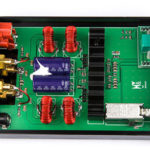
HV-50
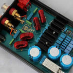
SA-50
The insides are a different story. Both use the same TDA7492 amplifier chip, but as you can see, the PCB and components are quite different.
Last night I noticed that one seller was offering the HV-50 for just $35 with free shipping, so I ordered one. At that price, it was a no-brainer. I’d have easily spent $25 and several hours getting one of the cheap TPA3116 boards I’ve ordered mounted in a suitable case.
I’ll follow up with a new post in a few weeks, once I have the HV-50 in-hand.
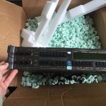
I recently discovered and purchased an inexpensive, unofficial WiFi-enabled AirPlay and DNLA audio receiver called the AirMobi iReceiver. I couldn’t find much information on the device, but for $12, I thought it was worth buying and trying.
It works reasonably well, but that’s not really why I bought it. I bought it with the intention of taking it apart and seeing what makes it tick. And now, having done that, I plan to hack it to run OpenWRT so I can secure it, customize it, and update the software.
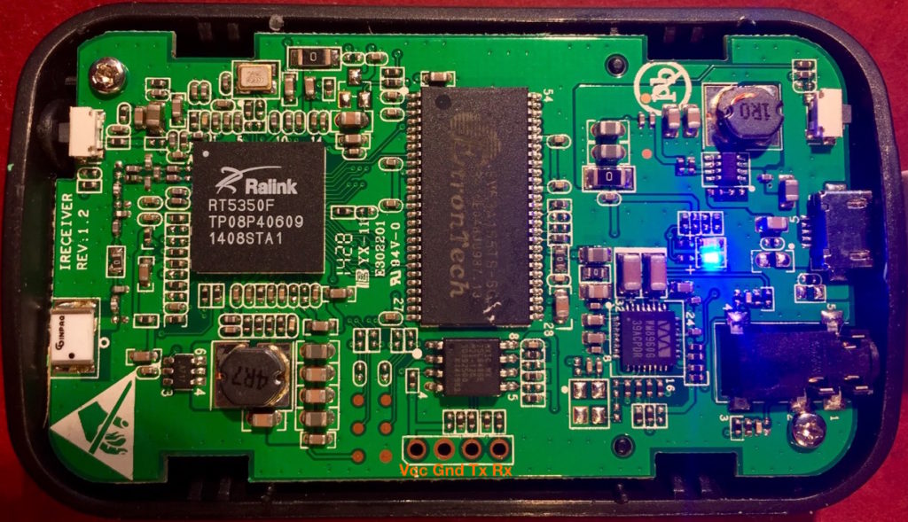
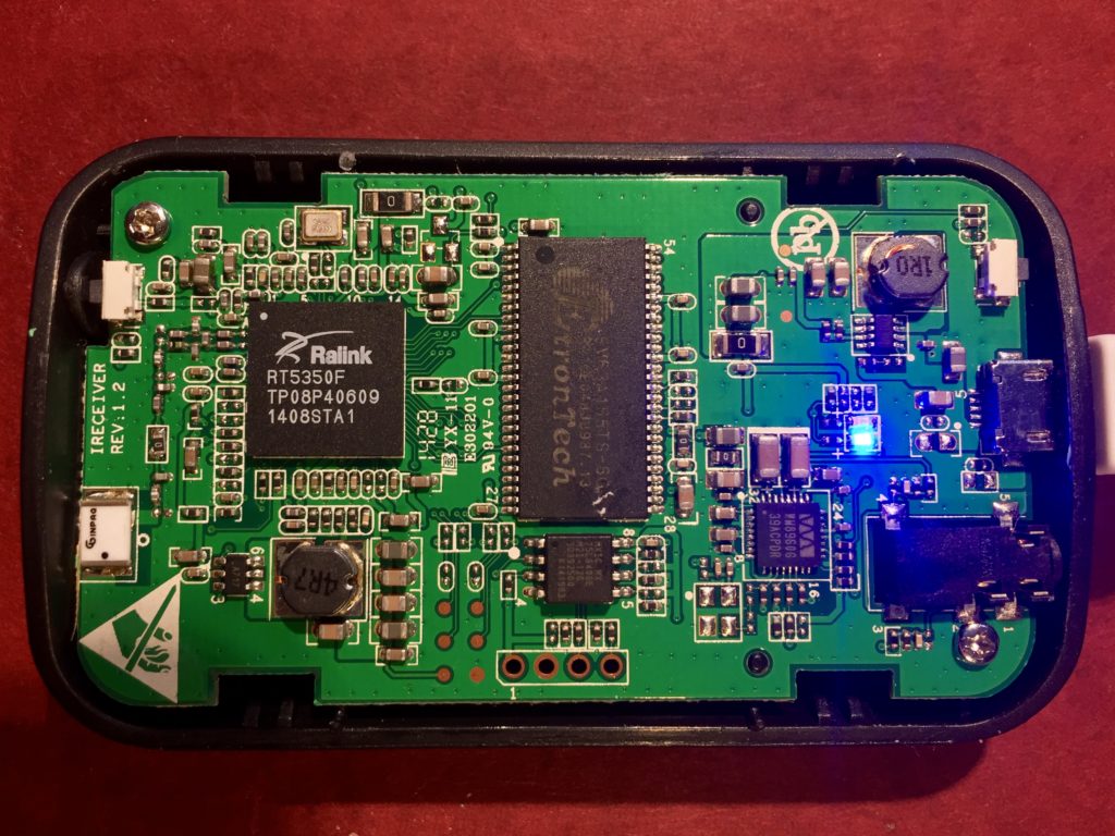
It is based on a Ralink RT5305T WiFi SoC which suggests to me that it is running linux, and probably has a serial console exposed via some test points on the mother board. I only found handful of candidates during my teardown. My guess was that the Tx and Rx lines were available on the unpopulated 4-pin header at the edge of the circuit board. From visual inspection I could tell that the second pin from the left was a ground pin. A little continuity probing with a multimeter suggested the first pin provided power, a fact confirmed when I check its voltage when I powered up the device.
I hooked a logic analyzer up to the other two pins to see which one toggled on and off at boot, but that was really overkill. I could have done just as well figuring out which one was pulled high when I powered up the device.
Once I had the pins worked out, I hooked up a TTL level USB/serial converter to my laptop, connected the ground pins and cross connected the Tx and Rx pins between the adapter and the board. Once I powered everything up, my screen started to fill with garbage. I guessed that 115.2Kbps was too fast, and tried 57.6Kbps instead. Bingo!
After booting up, I hit return and was presented with a login prompt. I tried the password for the webui and was pleased to find that it worked. I poked around the filesystem, looking at various config files, the various files for the web UI, and checking what binaries were installed on the system.
One of them is a telnet daemon (implemented as part of busybox). So, I started it, connected to the WiFi, and was able to log in over the network.
From there, I gathered more information. I was dissapointed that there wasn’t really anything like zip, or tar, or an ftp or ssh server that would make it easy to pull a bunch of files off at once, so I dumped the web UI files to the terminal one at a time and then saved them for further inspection.
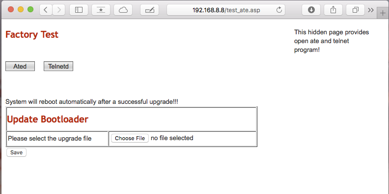
Hidden test_ate.asp page
Once I did, I found hidden functions in the firmware update page for uploading the bootloader over the webui. Exposing it required tweaking the page using web developer tools, which is kind of tedious. Then I hit the jackpot, I found an unlinked file called test_ate.asp. When loaded, it has a button to fire up the telnet daemon, making a command line available with just a WiFI connection, no serial console necessary. It also has an option to update the boot loader and a mysterious ATE function. This discovery made it easier to return and poke at the device at my leisure.
From what I learned in my poking and prodding, it appears to be based on the Ralink provided SDK with some modifications. With any luck, the modifications will be minor, and it will be easy to load an OpenWRT firmware over the webUI.
Before I do that though, I’ll need to take special care since this device doesn’t have an ethernet port, and so recovering from non-working firmware will be more difficult.
I’ve ended up with five small, inexpensive ($7-15 each) routers, running OpenWrt and only really need two of them, so I’ve been thinking of ways to use the others. One of my ideas was to get an external USB DAC, install Shairport-Sync, and use it as an AirPlay receiver for my car stereo, eliminating the need to connect an audio cable to my phone, and avoiding the mediocre sound quality of Bluetooth audio. It hasn’t quite worked out that way though…
While looking for an inexpensive (>$20), compact USB DAC with reasonable quality, I discovered there were integrated commercial products that already do what I planned to do. I already knew there were Apple-approved MFi-certified devices, but they tended to be expensive. I discovered there were cheaper devices using Shairport, but they tended to start at $30+.
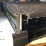
Damaged while trying to open the case.
With a little more digging though, I found a device called the iReceiver, from AirMobi that sells for as little as $12!!!. According to the scant marketing materials, it has a 24-bit Wolfson DAC. I was surprised I couldn’t find anyone who’d opened one up to see what was inside. I did find an Amazon review from someone complaining that the usb power connector had broken off on theirs, and the included photo showed it had a Ralink RT5350F WiFi SoC, which gave me hope that it would be hackable. So, I bought one.
Before opening it up, I tried it out. It works as promised. It defaults to broadcasting an unsecured WiFi network. Once connected, it shows up as an AirPlay receiver in iTunes, etc. From there, you can connect it to some powered speakers, select it and start playing music. The audio quality doesn’t suck (no obvious noise, clipping, or distortion), and in my limited use, there were fewer dropouts that I’m used to with Bluetooth.
Beyond that, there are various configuration options available through a browser based interface. There are no audio-related settings at all. Most of the settings are networking related. You can rename and secure the WiFi network with a password (good), WPS (bad) and by limited connections to specific devices by MAC address (meh). You can also connect to an existing network (good), and, optionally, extend it (meh). This seems like a good point to mention that it also works as a DNLA “renderer” (DNLA is a more open standard than AirPlay, making this useful to Windows and Linux devices, and Android phones with an appropriate app)
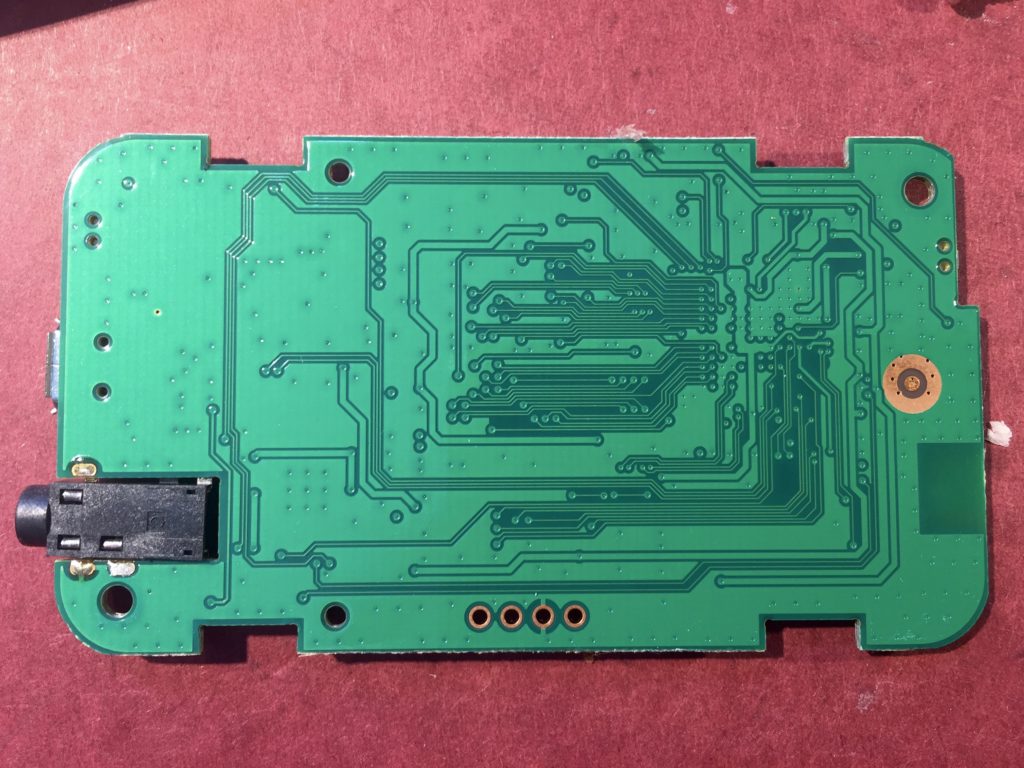
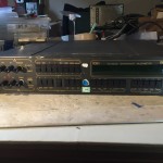
Of course, I didn’t buy it to use it with the stock firmware, so after trying it out, I opened it up to take a look inside. In the process, I managed to tear the translucent plastic that was affixed to the top of the case with adhesive. With the trim removed, it was easy to pry off the top, revealing the single PCB inside.
As I expected, it is based on the obsolete but inexpensive and popular Ralink RT5350F WiFi SoC which includes a CPU and 802.11n WiFi.
The other major component is a Wolfson WM8960 CODEC to provide the audio output. This chip debuted in 2006, and includes 24-bit stereo DAC and ADC converters supporting sample rates up to 48Khz, a 40mW headphone driver, and a 1W Class D speaker driver.
Despite being a 24-bit DAC, the specified SnR of 98dBS matches that of the 16-bit TI/Burr Brown PCM2705 DAC used in the original AirportExpress, rather than of a modern, premium 24-bit DAC used in more recent AirportExpress’s. Oh well. Good enough for my purposes. Most of what I’m playing is compressed AAC files derived from 16-bit sources, and, AirPlay only passes 16-bit anyway. Beyond that, the design of the rest of the circuitry matters, and I’m not qualified to analyze it, nor am I equipped or inclined to try and measure it.
Beyond that, I see two inductors on the board (one of which is cracked). My guess is that these are part of some small switch mode power supplies, perhaps one for the digital section, and the other for the analog. There are two small LEDs to indicate device status and two momentary switches, one to reset the device, and the other to trigger WPS. It looks like it uses a single ceramic chip antenna for the WiFi.
There are a few unused pads for components, eight test points (half seemingly to do with power) and four unused holes for pin headers that I suspect provide a serial console.
That’s really it for the hardware. I’ve already started poking more deeply into the software and investigating the suspected serial console, and I hope to have another post soon documenting what I found.
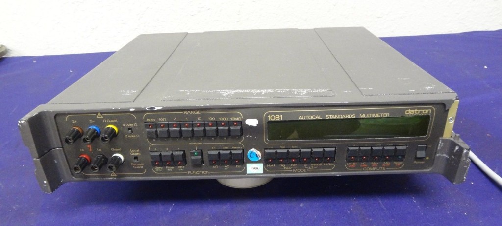
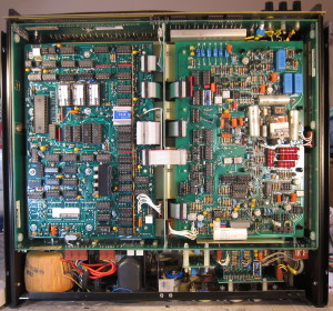
I’ve passed up a few chances to get a Keithley 2001 7.5-digit multimeter on eBay for ~$500, because while that’s a pretty good deal for a Keithley 2001 in working order, it’s more than I can justify spending on a 7.5 digit multimeter that I want, but don’t need. Somehow though in my twisted psychology, spending $300 on a two-decade older 7.5-digit multimeter with known issues is perfectly acceptable, because I recently did just that.
A couple of weeks ago, I was checking eBay on my phone while waiting for an appointment and came across a new llisting for a Datron 1081 Multimeter that caught my eye. It was listed for parts or repair for $300, or best offer.
According to the description, it had been damaged in shipping, and gave an error during selftest. From the photos, it looked like the shipping damage was confined to a broken “ear” on the front of the case, and misalignment of the front panel. Definitely interesting…
Some quick googling confirmed that the 1081 was, as I thought, a 7.5-digit capable multimeter with high stability and and the ability to use an external voltage reference. I thought it would be useful for evaluating and calibrating precision voltage references, and 6.5-digit DMMs, like the Keithley 2000 and HP/Agilent/Keysight 34401a. I couldn’t find an operators manual for the 1081, but I hoped the 1071 manual I found was correct that the selftest error was with the AC measurement circuitry. I’m mainly interested in DC, so I wasn’t too concerned.
I reviewed past eBay listings on my phone to confirm that the 1081 typically goes for more than $300, checked my gut, and decided to make an offer of $200.
The seller responded within a few hours that the listing had generated a lot of interest, and counteroffered for $275. At this point, I was back home, with the ability to browse eBay without the limits of a phone. I should have taken advantage of this to investigate past listing a little more thoroughly. If I had I would have realized that some of the higher sales prices weren’t actually sales, they were expired listings that eBay wasn’t filtering properly. I didn’t though, instead I accepted the offer.
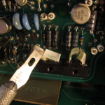
It took a few days for the seller to ship the item, and it was shipped by FedEx Ground, so it took over a week to get to me. It arrived last Friday, packed well in a Cisco router box with reused foam endpieces and packing peanuts for extra protection. It was in the physical condition I expected; the case damage was limited to an extremity, and the main enclosure was sound. I opened it up for inspection and to deal with the misaligned front panel.
The front panel is a metal plate covered with a big printed plastic sticker. The sticker holds a smoked plastic protective lens over the display. The sticker was loose at a few spots, including the protective lens, which allowed dust and exposure to further weaken the adhesive. I decided to remove it, clean it up, and reattach it.
I heated the panel with a hair dryer to loosen the adhesive, but that didn’t work all that well. I ended up peeling the outer layer and printed layers of the sticker off its backing. Some adhesive remained on on the printed surface of the label, and the backing remained stuck firmly to the metal plate. I used a plastic scraper to remove most of the backing, but getting the rest off required a razor blade, elbow grease, and solvents (“Goo Gone” worked best). I used isopropyl alcohol to clean the remaining adhesive off the back of the printed sheet. Unfortunately I think the process of peeling off the label led to some of the printed brown background along the left side of the lower edge crazing and flaking off. I considered trying to apply a new background of spray paint, but decided the risk of causing further damage wasn’t worthwhile.
Once I got everything cleaned up, I decided to use some non-corrosive silicone adhesive to stick everything back down again. I smeared a thin layer all over the back of the sticker, and around the edge of the smoked lens before lining everything up and sticking it back down, smoothing it out and wiping off any ooze. I weighted the area over the lens and let it cure for a few hours before reattaching it.
Top
Bottom
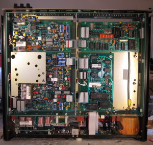
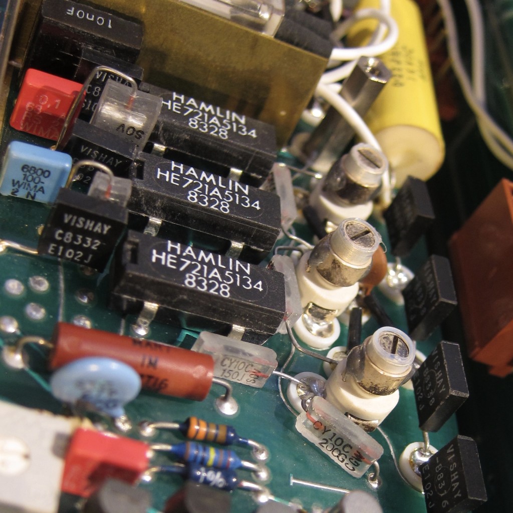
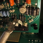
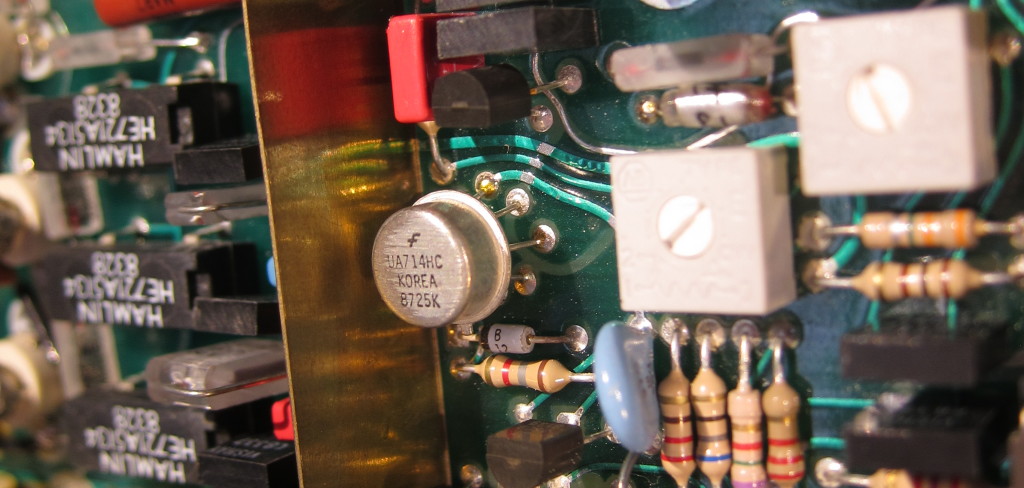
As for the electronics, there sure are a lot of them, and very few of them are electrolytic capacitors – the component most apt to fail on older equipment. I looked everything over very closely.
I was relieved not to spot any physical problems, because while everything is through-hole components, many of them are packed in very closely, and a number of them look like nothing I’ve ever seen before. Repair would be challenging.
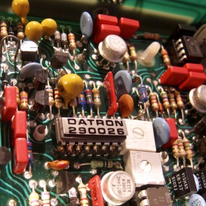
My first Glass Capacitors
Actually, there was one problem, but one I expected to find.
The back panel was labeled at manufacture with a battery replacement date of April 1992! Either the battery hadn’t been changed, or whoever did so was too lazy to update the label. Inside I found the truth, the battery had a datecode of 1984, like most of the other components. Fortunately it still had a voltage of 3.7v, but I’ll be changing it soon.
I found a few other interesting things as I looked the device over.
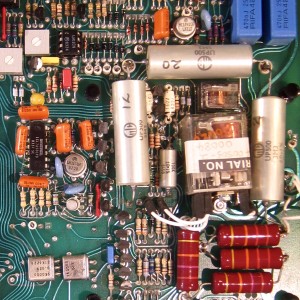
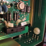
The photos above feature four 1N829a temperature compensated zener diodes. Together, they make up the heart of the voltage reference. They are each numbered with a unique serial number because they were carefully aged for months (or years), then characterized for noise, stability, voltage, and the current at which they have flat temperature sensitivity. My understanding is that the four Zener are connected as two parallel series of two.
I plan to look at these in more detail in a future post, because the unique characteristics of this voltage reference may make it the most notable part of this device. The use of hand-selected temperature compensated Zener was a common practice in a variety of precision instruments at one time, even so, the use of multiple TC Zeners was unusual, as is the stability they obtained. Also by the mid-1980s, when this device was made, use of temperature stabilized burried-Zener voltage references, like the LM199 (introduced in 1976) was commonplace.
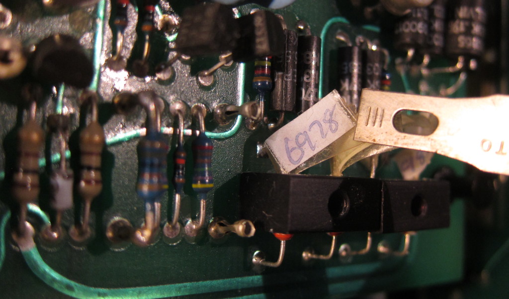
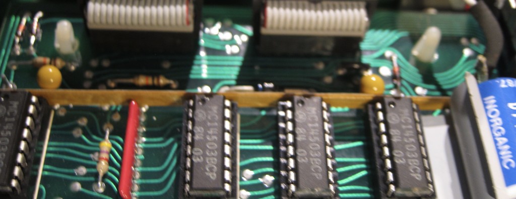
This insulated metal strip running the length of the digital board between a row of I/O bufferes, and the ribbon connectors, also caught my eye.
I found evidence of a component level repair on the AC RMS converter board. Most of the components on the AC RMS converter board, and most of the other boards, have date codes no later than mid-1984, but the Fairchild opamp in the hermetically sealed package in the photo above is dated from 1987. The GPIB board seems to date from 1985, and there are some socketed ICs on another board that have 1986 date codes, while other chips on the board are from 1982 or 1983.
Artifacts of repair can also be found on the inside of the case, where some of the melted nubs holding the RF shielding seem to have sheered off and been replaced with some glue.
Functional Tests
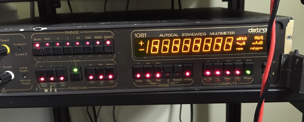
After checking it over and fixing the front panel, I reassembled it, and powered it up. On the EEVBlog forum, “dacman” suggested that self-test error could simply be the result of running the tests with the “guard” switch was set to remote. I could see from the photos on the listing that it was, indeed, set to remote, and it still was when I received it, so I set it to local guard and ran the self tests. Everything passed!
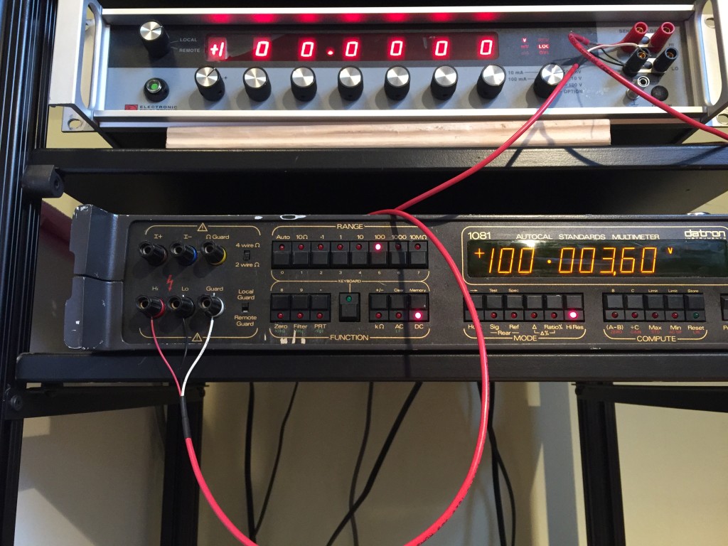
After that, I did spot checks on the 100mv, 1v, 10v and 100v DC ranges using the output from my EDC 521 DC voltage calibrator. The EDC hasn’t been calibrated in years, though from my tests, it is accurate to within the combined 1year tolerances of both it and all my 6.5 digit DMMs. The readings are stable over the short term.
I’ve also done some longer term checks of a 10v signal over a period of days and found that for the most part, the peak-to-peak variation is within the 20-40uV range measured by one of my Keithley 2700s (it is a 6.5-digit meter, but in stats mode it collects and calculates 7.5-digit values) in my Seattle home, near an external wall, without any heating. Sometimes the Datron has reported a wider range than the Keithley, sometimes a narrower range. I’ll need to get logging working over GPIB soon so I can can look more closely at the trends.
Unexpected behavior
In the first few days, of use, I ran into a few instances of unexpected behavior, some of which may have been user error, some of which may have been software bugs, and some of which is as of yet unexplained.
One of the first things to crop up happened while I was checking the 100v range with a 100v output. After the initial readings seemed good, I left it for a while and checked it while I worked. About 15-30 minutes in, I looked over, and it was reporting values of 110v or more, and they were changing quickly. I haven’t been using the EDC much in its 100v range, so I breifly considered the possibility that it was at fault, but a quick look at the Keithley 2700 measuring the same source showed that the voltage was still stable at 100v.
The reading on the Datron was still on the move and soon it was reporting an “Overload.” I tried changing to the 1000v range, but the Overload message remained. I cut the EDCs output and after about 30s, the Datron cleared the overload message and started giving readings again. I applied an input again (I can’t remember if it was 10v or 100v), and it again gave plausible readings. I left it for a while and continued checking it, and after a while, it was again reporting an overload. This time cutting the EDCs output didn’t clear the overload message, and I ended up power cycling it.
Since then, I’ve been focused on the 10v range, and I haven’t seen this behavior again. I have had it with a 100v input for the last 18 hours or so though, and its been solid. I’m beginning to suspect that the problem may have been the result of user error. At some point, I think I’d used a function that “zeros” the meter. I thought this worked like the relative measurement option on my Keithleys, which can give readings relative to any voltage. The Datron 1081’s feature is different. The zero-point is supposed to be set with the inputs shorted, and the value is stored and used until the next time the meter is zeroed. If it is more than a small portion of the full range (1% or so), it will give a overange error. I’m wondering if perhaps the zero-point that I or someone else previously set was near the limit, and perhaps some internal auto-correction ended up pushing things over the limit. This is just a stupid wild ass guess though. All I can be sure of is that since setting the zero point for all the ranges with the input shorted, I haven’t had this happen again.
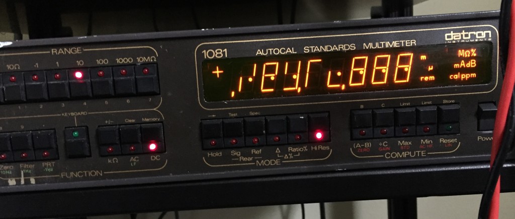
I spotted the next problem after leaving the DMM on overnight. When I checked it the next morning, I suspected that the display had frozen because the last digit didn’t change once. I pushed a button to change the value displayed, and was treated to the above, after a minute or two, it seemed to reset itself and resume operation.
The next morning, after leaving it overnight, I again found it with a frozen display. The first button I hit produced a similar result to the previous day. I tried hitting another button (I don’t remember which) and the rest of the display segments and all the indicator LEDs on the buttons lit up too. This time, it didn’t reset itself, at least not before I got tired of waiting.
I haven’t seen this behavior since, despite leaving the unit on continuously. A few days ago though, I decided to investigate a hunch. I thought that that when I saw this problem behavior previously, I may have left the unit displaying the delta between minimum and maximum values. So, I again left it in that state, and the next morning, the display was again frozen. This suggested that my memory was correct, and that it was infact a software problem. However, the following morning, after again leaving the unit in min-max display overnight, the problem didn’t present itself. So, it seems that I still don’t have it figured out.
What Next
I’m trying to decide where to go from here.
At the very least, I’m going to power it down, open it up again, and take a close look at power supply voltages and ripple.
When I power it up again, I’ll keep an eye out for a recurrence of any of the bad behavior I observed. If so, it will suggest that some of the problems are the result of bad solder joints that act up when the unit is coming to a new thermal equilibrium.
Beyond that, i’ll do some logging over the GPIB interface to get a better sense of stability and tempco. I also need to investigate the resistance and ACV functions.
After that, I’ll have to consider whether to get it calibrated, or figure out a way to calibrate it myself. I’d also like to investigate its ability to use an external voltage reference to provide high-precision comparisons between different voltage standards. Doing so will require either figuring out a source of the (likely expensive) low-thermal-EMF rear panel connectors, or replacing them with similar performance and lower cost.
I’m also still looking for a Datron 1081/1082 Users Handbook (the 1082 is basically a 1081 with all the options). The Datron 1051/1061/1071 users handbook has been useful, because for the most part, they operate very similarly to the 1081, but there are some important differences with the digital filter, and some of the other aspects.
The kit makes use of through-hole components for easy home assembly. It includes an external 8MHz crystal, a voltage regulator, and uses narrow 1% and 0.1% tolerance resistors in critical positions for highest accuracy.
The case is designed to use a ceramic socket (provided) for connecting components, and also provides two banana jacks to allow test leads for testing larger components. People have complained that the provided socket is hard to use and doesn’t make good contact, and I wanted all three test connections available via leads, so I decided to modify the case.
My modification is inspired by some of the fully assembled versions of the tester I’ve seen on ebay. I cut a piece of plastic and glued it over the existing holes for the socket and banana jacks on the case and drilled three holes for 2mm banana jacks I ordered on eBay. Then, I cut a piece of protoboard and drilled three holes for some 2mm banana plugs, which I screwed into the board. Then I soldered in the ZIF socket and connected up the leads to the plugs.
I haven’t tried building the latest firmware from source for this, but my understanding is that “mega328_st7565_kit” is the proper version to build.
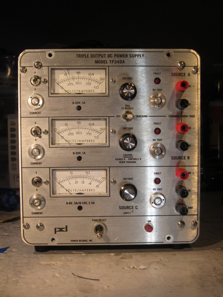
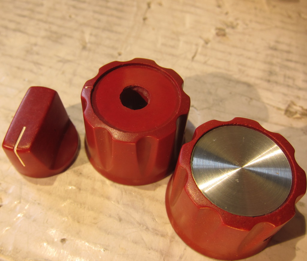
My Power Designs TP340a bench power supply has a look and feel of quality stemming from its industrial design roots in the 1960s. Unfortunately, my supply was built in the mid-1990s and the design was compromised by the use of plastic knobs for the voltage controls on each of the three independent power sources.
TP340a with “original” plastic knobs.
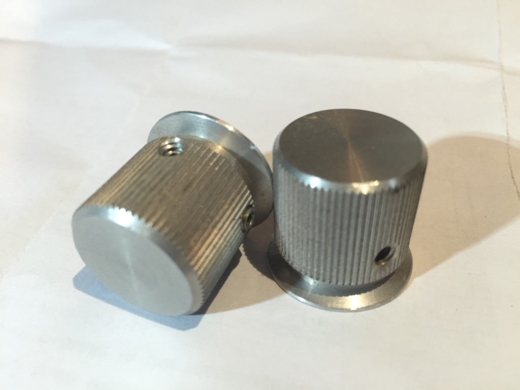
Since getting the supply up and running, I’ve been on the look out for some suitable replacement knobs. Other/earlier models of these Power Designs power supplies appear to have used knurled aluminum knobs supplied by Kilo International. Kilo sells similar knobs to this day, but they apparently long-ago discontinued the model Power Designs used (which is probably the reason for the substitution in the first place).
In the current lineup, Kilo has two lines that might serve as suitable substitutes. The JD series has the right overall profile, with a flat top rounding into a straight side, but it lacks the flared skirt of the originals. The DDS series has the skirt, but the rest of the profile isn’t right, with a flat top dropping to a flat side that then flares slightly for the knurling.
I suspect that the original knobs were a skirted variant of the JD series, probably called JDS. I scoured eBay for old stock or used knobs, without luck, but I did find a seller with used knobs of similar design. In fact, they look like knobs that Power Designs used on a number of supplies made in the late 60’s or early 70’s. The price wasn’t bad either, 5 knobs for about $17, shipped.
They still weren’t quite right though. The fact that the design wasn’t an exact match wasn’t the issue. Rather, I was concerned that they were a little wider than the original knobs, and that their proportions would seem off (I lack the skill to create a nice, well proportioned design, but I can tell when things are off). Because of this, I dithered on ordering them, but after seeing his stock decline, I finally pulled the trigger.
The knobs were in pretty good condition, other than being a bit gunked up. I gave them a washing and scrubbed them gently with some Barkeepers Friend (a mildly abrasive cleaner for glassware and stainless steel) before replacing the existing knobs.
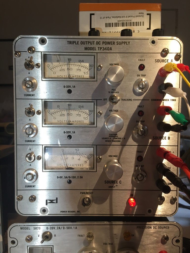
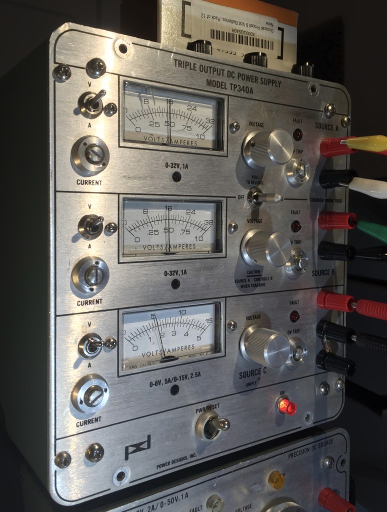
I think my concern about proportions were warranted. The I think the knobs give the supply a bit of a big-nosed look. Still, I think they look better than the plastic knobs that it had before, and the definitely feel better to use.
The seller also offered some knobs with the same design but a smaller diameter. I would have purchased them instead, but for the fact that they were drilled for small diameter potentiometer shaft. I considered getting them and drilling them out, but I don’t really have the right tools and so I figured it would be a frustrating project that I could do without right now.
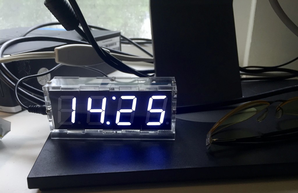
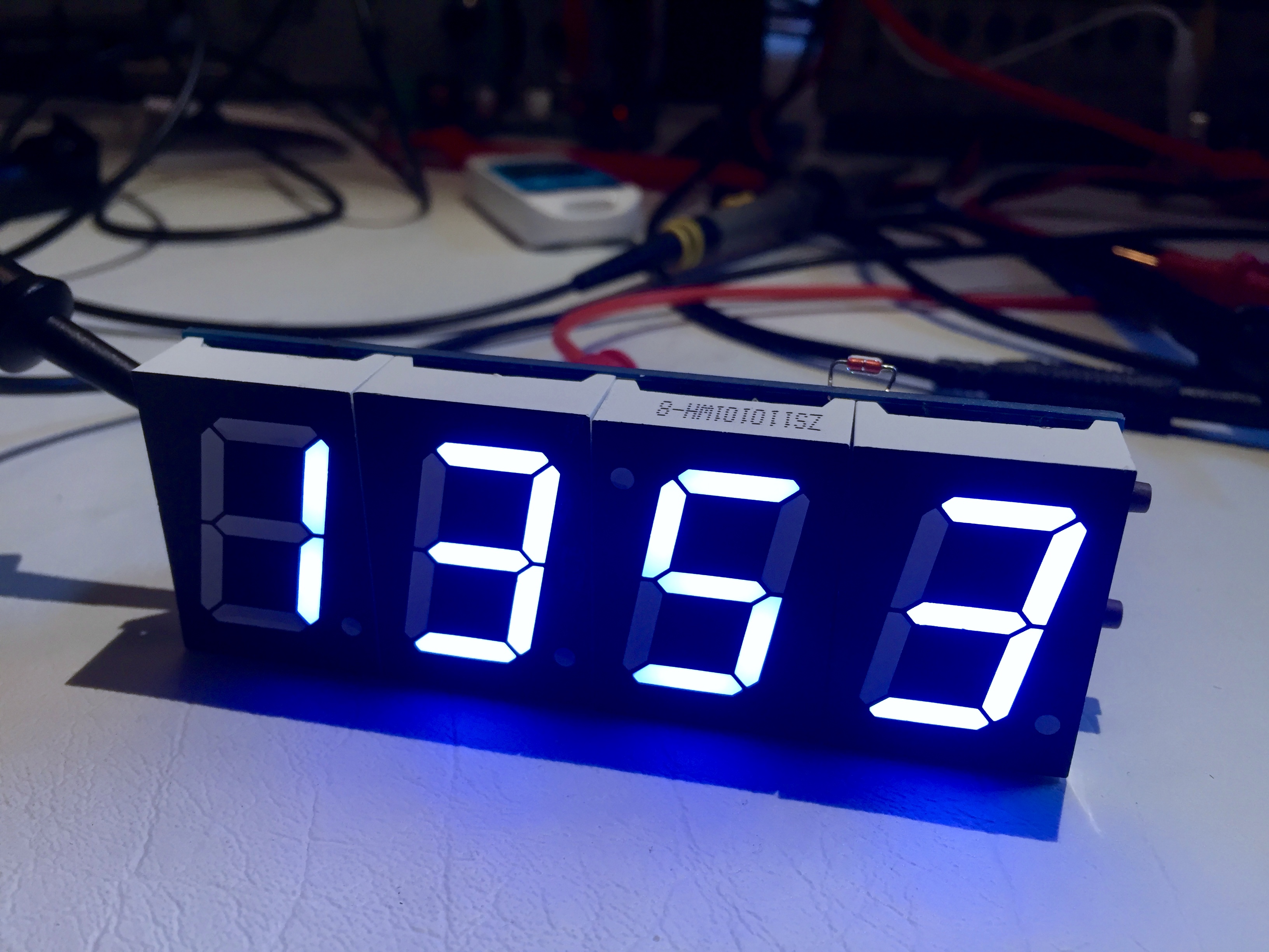
A couple of months ago I was browsing Banggood and came across a stupid little clock kit that I felt drawn to for some reason. I suppressed the urge, but not before seeing if I could get the kit for cheaper on eBay (I couldn’t).
About a month ago, I was looking at Banggood again, and this time I gave into temptation and ordered the kit and it finally arrived, by way of Sweden!! a week or so ago and I assembled it yesterday.
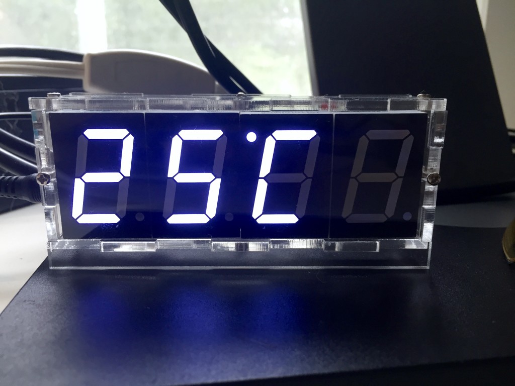
I’m still not sure why I was so attracted to the kit, even now that I have it assembled and working on my desk, but I have an idea. I think a big part of the appeal is the minimalism of the device. From the front, all you see is the inch high LED digits. The circuitry is all on a board hidden behind the LED modules. The optional clear acrylic case is similarly minimal. It’s just six pieces of clear acrylic, with tabs and notches cut to interlock, holes for the six screws and slots for the six nuts that fasten it all together.
Features:
1″ white digits (other colors available)
Clock (24hr/military time only, so far as I can tell)
Temperature, Centigrade only, alternates with time display
Alarm
5v power with cord for powering from a USB connector
Battery backup for the clock.
The kit comes with all the thru-hole parts needed to assemble the clock and 8.5×11″ sheet of paper with the instructions printed on one side. The instructions are probably enough to build and operate the clock given some basic familiarity with assembling electronics, which is not to say that they couldn’t be better.
Assembly
Assembling the kit is quite simple. There are about two dozen resistors of three different types to be added to the board, along with a with a diode. After placing and soldering these low-profile components, I added the six provided solid capacitors and the crystal, then the two IC sockets, six transistors, pezio buzzer, electrolytic capacitor, power socket, switches, and a surface mounted coin-cell holder.
The transistors proved just slightly tricky, because the provided transistors are in a TO-92 package, while the PCB is layed out for something with a wider lead spacing like a TO-126. The solution is simple, bend the leads to fit, but it’s a bit fussy.
Before finishing soldering the components, I partially assembled the case so I could check the distance between the back of the board and the notch cut in the case to provide direct exposure to the thermistor. Photos of the assembled clock on Bangood show the thermistor sticking out high above the case, which strikes me as ridiculous and unnecessary. I decided that ~1cm off lead between the board and the component was enough to position it in the cutout while remaining protected by the case. I bent the leads to be parallel to each other and perpendicular to the axis of the thermistor package, then 1-2mm from that bend, I bent both leads at another right angle, so the leads remained parallel in the same plane, and the thermistor was a elevated slightly above it. I then soldered the thermistor to the board so there was about 7mm from the PCB. I did something similar for the photoresistor, so it could face upward. I bent the leads a couple mm away from the package, and then soldered the leads so they protruded about 5mm from the board.
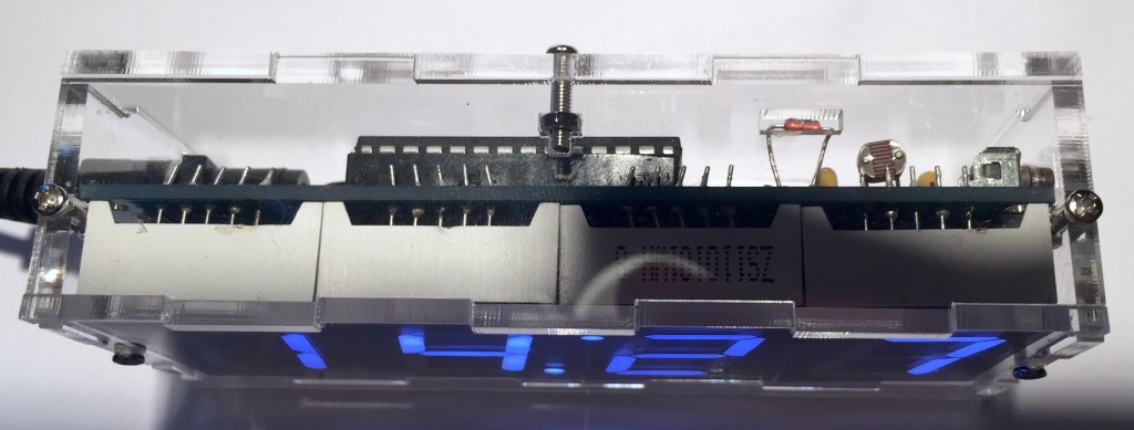
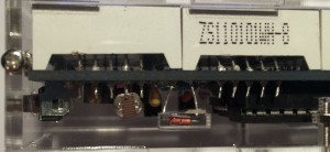
Once the components were all soldered, and the leads trimmed, I checked over the board and fixed a number of dodgy solder joints before adding the four 7-segment LED modules on the opposite side of the PCB.
The third digit brought unexpected difficulty. It is supposed to be rotated, so that the dot that usually sits at the lower right to serve as a decimal point, will instead sit at the top left, to serve as the top dot of a colon separating hours from minutes formed with analogous dot at the bottom of the previous digit. This rotation presented a problem, because the leads at the top and bottom edge of the LED packages are offset, rather than centered, and the PCB wasn’t laid-out to account for this. All the leads had to be bent to accommodate. Again, a relatively simple task, but fussy in practice, because of the need to maintain the spacing between the 5 leads on each side so they will slip into the holes on the PCB.
Troubleshooting
At this point, I fit the ICs to their sockets, powered up the clock, and found that it worked. Or should I say, mostly worked? The left-most digit didn’t light up. I tried resetting the device as described in the instructions, but it still didn’t work. I checked all the solder joints for the LED module, and they seemed Ok, but I touched some of them up with another pass of the soldering iron. I also consulted the schematic to figure which transistor is responsible for strobing the power to the module and checked/touched-up its leads. The first digit still wasn’t lighting up. It was time for bed.
After a good nights sleep, and breakfast out with friends, I returned to troubleshooting the clock. I spent 15 minutes or so using the continuity function on one of my multimeters to trace out part of the circuit and better associate the schematic with the actual layout of the PCB. In particular, I was interested in the portion of the circuit responsible for powering the problem LED module. I figured out the center pin on either side of the module provided +5v, and that there seemed to be good continuity between that and the collector lead of the controlling transistor (Q1). I also found that there was proper continuity from the base of the transistor to the associated resistor, and that the other end of the resistor was, indeed, connected back to an output pin on the microcontroller. Finally, the emitter was properly connected to the 5v supply.
Since everything seemed to be connected properly, I needed to look elsewhere to figure out why the clock wasn’t functioning properly. I thought, perhaps, one of the components was defective. Rather than going to the trouble of testing them individually, either in or out of circuit, I decided to power up the device again, and use an oscilloscope to inspect the signals at various points in the circuit, and compare them against the signals at analogous points for the other functioning digits. This would help me pinpoint the component in need of attention.
That was the idea, anyway. Once I powered the clock up again, the problem digit lit up. I’m not sure what happened. Perhaps my probing and shifted a faulty solder joint back into contact? I tried pushing on a few spots, to see if I could reproduce the problem, but nothing happened. In the end, I decided I had better problems to solve than chasing down an intermittent fault in a $12 clock kit, mounted it in the case, and called the project done.
Other Details
The PCB has some unpopulated areas. The documentation doesn’t say much about them, other than that they are “DIY” areas and no components should be installed. The schematic casts some light on what they are for. There are some headers for in-circuit-programming, and another which, I think, may be for resetting the MCU. There is also space for a relay, and an accompanying space for a connector/header for attaching the switched load. Given the design and clearances on the PCB, and the width of the associated traces, I’d guess that it is only suitable for switching low voltages at modest currents (~1A, tops). The firmware also seems to support this relay by allowing you to set an our to turn it on, and and hour to turn it off.
For what it is worth, the device uses a pre-programmed STC15F20EA_28 microcontroller in a DIP package. This MCU comes from STC Micro, in China. It has an implementation of the 80C51 CPU, along with 4K of flash, 256 bytes of SRAM, an 8-channel, 10-bit AD converter and 1K of EEPROM. This chip isn’t particularly hobbyist friendly, other than being inexpensive. Someone did create software for programming these chips called ‘stcdude.’ It is analogous to ‘avrdude’ used for programming Atmel avr microcontrollers. You’ll also need a compiler like SDCC (small device C compiler). That, and experience doing embedded development without much handholding. This isn’t an Arduino, nor is it Arduino compatible.
The MCU is complimented by a DS1302 clock chip (or something that functions like one), which stores the alarm settings, and keeps time on battery power when the external power isn’t connected.
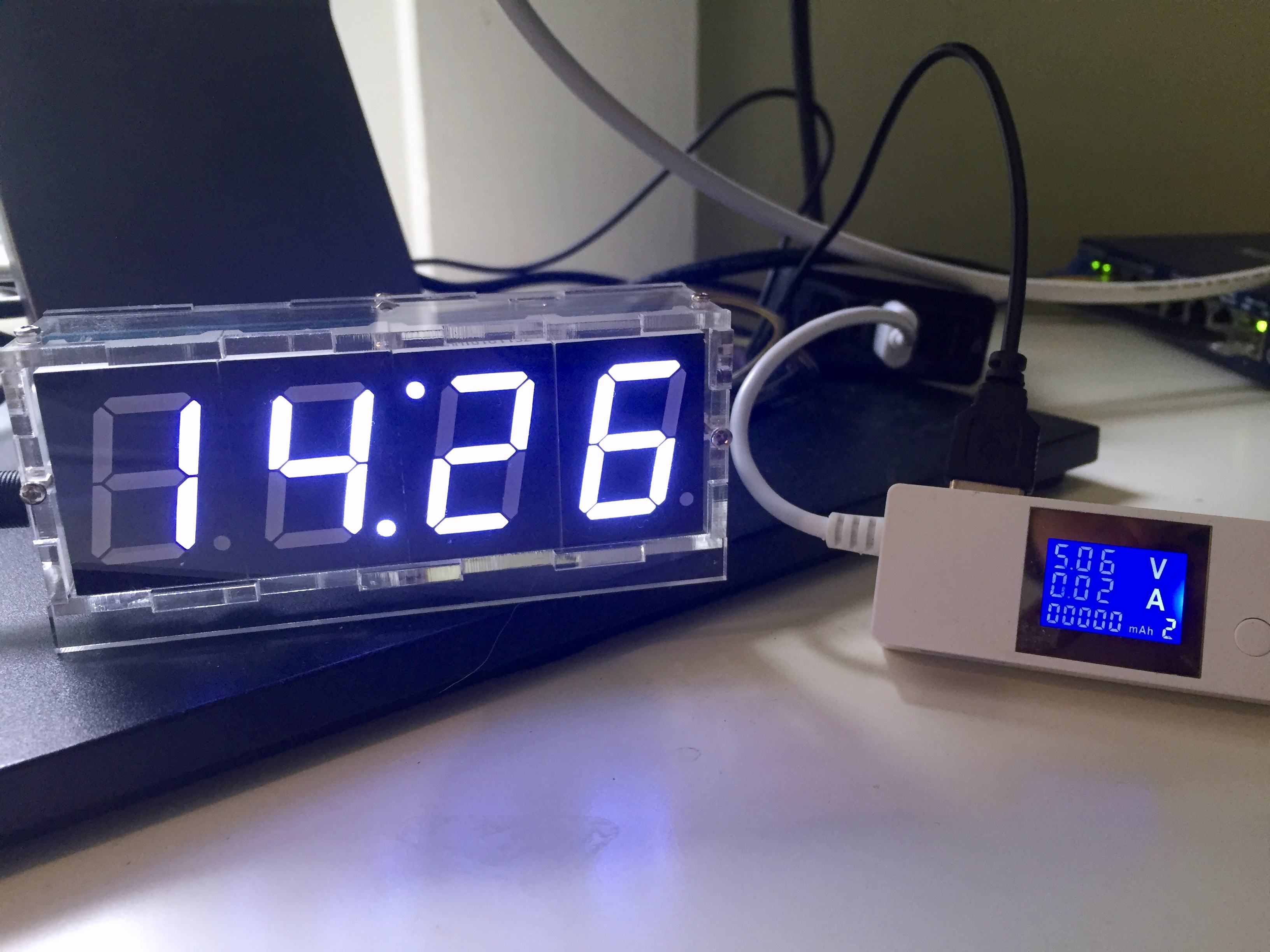
I measured the power consumption using a USB meter, and it read 0.01-0.02a, or 10-20mA. In theory, you could probably run it for ~4 days off of a modest single-cell USB powerbank. In practice though, it probably doesn’t draw enough current to keep most USB power banks switched on.
Conclusion
I’ll give this kit a solid B overall. The kit and instructions are a B- because of the layout problems I mentioned above. The finished product is a B to a B+. It think it is attractive, and useful, but as an American, the fact that it only displays time in 24-hour mode and temperature in Centigrade undermines its utility somewhat.
I should also say that while the temperature seems accurate to within a degree or so, I have no idea how well it will keep time.
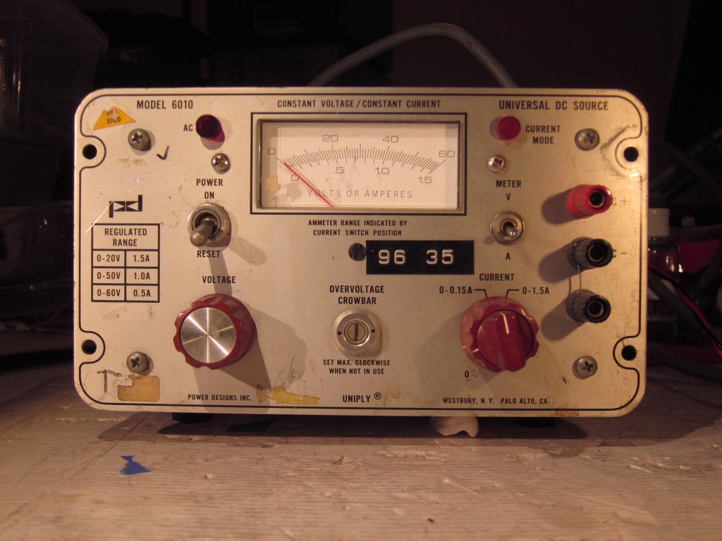
A couple of weeks ago I came across an listing for a used Power Designs 6010 for just $20, shipped. At first glance I thought I’d come across an incredible deal on a 6050, because the 6010 looks very similar. I’ve been keeping an eye out for a deal on a couple of Power Designs 6050 supplies for a while, with an eye to running them in parallel to get 10A for use in calibrating some battery testing equipment. It was disappointing to realize it was a 6010 a 60v/1A supply. I can already cover that voltage and current range in a couple different ways with existing equipment. I bought it anyway, because $20!!
The seller took his sweet time shipping it out, but I finally got a tracking number, and a few days later, the supply arrived, well packed, and in, outwardly, pretty good physical condition. Inside was another story.
One side of the PCB looked great. The other side though…
Absolute crap. The PSU clearly had a thick layer of dust inside before receiving a light sprinkling of water. I set about trying to clean it up. I got two bowls of fresh water and a toothbrush. I wet the toothbrush in one bowl and I scrubbed the PCB with it. When it was too dirty, I rinsed it in the second bowl, then wetted it again from the first. After 5 minutes or so, the board was looking much better. I followed up by soaking it with squirts of 70% Isopropyl Alcohol (IPA), letting it run of onto a paper towel, and then chasing more if off with some compressed air. I repeated the process again with more 70% IPA and then with two rinses of electronics grade 99% IPA.
After cleaning the board looked much better, and I could see that the corrosion that had started was superficial.
While I waited for it to dry out fully, I carefully inspected all the components. All the components on the front-side of the board looked in good shape. The big electrolytic caps on the backside of the board showed signs of leaking small amounts of electrolyte, but they tested out Ok with the capacitance function on my multimeter. I followed up my hooking each one up to one of my other bench power supplies and monitoring the current while I gradually raised the voltage, looking for signs of high leakage. Then I disconnected each cap from the PSU and checked how gradually the voltage dropped. None showed obvious signs of misbehavior. I plan to replace the caps, but I decided they were good enough to use while I did further checks on the supply. Before proceeding to functional checks though, I cleaned up the knobs and the front panel.
The knobs are red “Daka-Ware” resin knobs. Daka-Ware is/was a brand of products made with a thermoset resin, similar to Bakelite. Like Bakelite, there are various fillers mixed with the resin. Over time, the resin and filler age at differential rates from physical ware, and exposure to UV light, oxygen, pollutants, and dirt and grime. The knobs on my power supply had an obvious dull, darkened patina to them. When I removed them, the previously covered areas were still bright and glossy, making the wear even more obvious.
Next I washed the knobs with mild, soapy water. This removed a fair amount of the dark grime, but when they dried, it the knobs seemed lighter, but still dull due to the layer of partially exposed filler. Some people address this problem by painting the knobs, which to me defeats the purpose of making them out of colored resin in the first place. Others buff and polish the surface until they get a smooth surface of fresh resin, but that can end up removing a lot of material. I rubbed the knobs gently with a wet melamine sponge to remove a thin coat of exposed filler and aged resin. Once the knobs dried, I covered them with a generous coat of carnauba wax in order to impregnate and protect the remaining exposed filler, and the resin underneath. I then polished the knobs with a soft cloth.
The results aren’t perfect, but they are pretty good. I’ll probably put another couple coats of wax on before I call it done.
As for the functional tests, well, I’ll save that for another post.
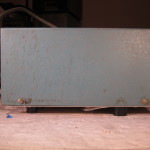
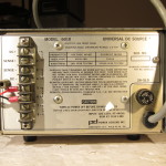
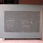
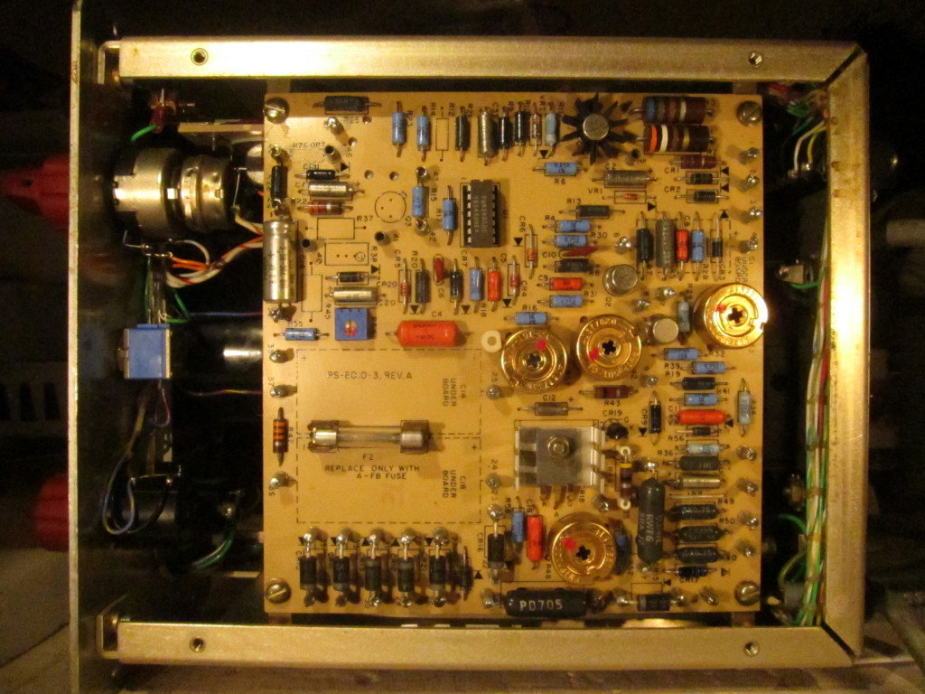
Last week, I cleaned up the used EDC 521 DC Voltage & Current Source I bought on eBay and ran it through some quick tests. The next day, I connected it up to one of my Keithley 2700 6.5 digit multimeters, started logging readings, and powered it up. Since then, I’ve been collecting voltage readings every 5 seconds so I could get a better sense of the device’s stability and accuracy.
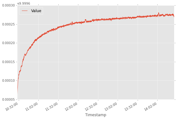
The EDC 521 was set to 10.00000v and powered on.
Once the self-tests ran the output turned on. The initial voltage was only 9.99954v, but climbed quickly. After 15 minutes, it was up to 9.99981v and still rising gradually. At the end of the specified two hour warm-up period, it was 9.99986v, well within the specified tolerance of 0.000258v (0.002% of setting + 0.0005% of range + 3uV), as well as the DMMs uncertainty of 0.000350v 30ppm of reading + 5ppm of range.
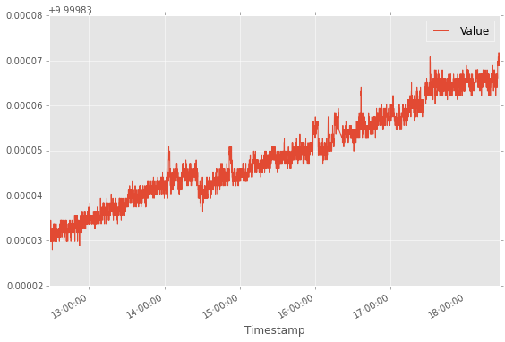
After the initial warm-up, the voltage continued rising for another 5 hours, before leveling out at about 9.99989v.
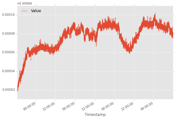
The graph above shows the voltage over ~4 days following the two hour warm-up period. If we look at the stability once the voltage first leveled out ~7 hours after turn-on, we see that it lies between 9.99990v and 9.99994v, which works out to be about 4 parts per million (ppm), which is better than the specified 7.5ppm 8-hour stability and the 10ppm 24 hour stability for the source and ~14ppm 24-hour stability of the DMM.
I’d guess that some of the variation is due to temperature changes. The EDC 521 specifies a temperature coefficient of +- 5ppm/C°, and the DMM has a temperature coefficient of about 2ppm. Unfortunately, I didn’t start collecting temperature readings until yesterday afternoon. Once have accumulated a few days worth of readings, I’ll look at the relationship between temperature than the voltage reading.
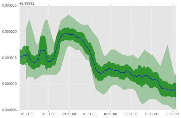
The last thing I did was look at short term variation in readings. The graph above looks at a 4 hour period earlier today. The blue line is a moving average of 10 minutes of readings (~120 readings), the dark green shows the standard deviation in readings over the same window, and the light green bounds the average of the minimum and maximum readings over the same period.
It shows that the difference between minimum and maximum readings are ~6uV, which is less than 1ppm. The DMM is only a 6.5 digit DMM, which means that the smallest reading on the 10v range is 10uV. When readings are taken using the GPIB or RS-232 interfaces, it does report an extra digit, which is useful for statistical purposes. In this case, I think its safe to say that the short term variation in readings is probably mostly down to the DMMs noise floor.
After looking over this data, my conclusion is that I got what I was hoping to get, a stable and accurate precision voltage source. Next step is to test the GPIB interface and use it to collect data across every available setting and range to check for linearity/accuracy and decide whether any adjustments are needed.


