Today I updated the firmware on my GL-Inet MT-300N v2 “Mango” travel router, and while I had it out I decided to measure its power consumption.
For those who don’t know, a travel router makes it easier to securely use a temporary internet connection, like that provided by a hotel, and share it among multiple devices. The hardware specs on the GL-MT-300Nv2 are modest, but sufficient, it is compact (about the volume of a deck of playing cards), and inexpensive ($20.49 on Amazon). The firmware is based on a recent release of OpenWRT with a UI optimized for use as a travel router. For those who want it, the standard OpenWRT Luci interface is available.
I decided to test the power consumption because my tiny solar power station (~18W panel, 120Wh LiIon battery), was generating more power than it could store and I’d already finished charging my phone for the day. As I unplugged my phone’s charging cable, I noticed that the USB-powered router was right there, so I plugged it in instead and reset my USB power meter.
Once the router started up and I connected my laptop to it over wifi, I noted the power consumption was about ~1.3-1.5W. I ran an Internet speed test from my laptop and the power consumption bumped up slightly. After an hour, the cumulative power consumption was ~1.4Wh. I connected the router to ethernet to see if that made an obvious difference in the power consumption; it didn’t.
Based on these crude measurements, I think it’s safe to say that the GL-Inet GL-MT-300Nv2 uses less than 2W on average. That means that, if necessary, it could run for >3h off a typical small USB power bank, and could probably run directly off a ~$15 6-7W solar panel with USB output through most of a summer day.
I didn’t check the power consumption while using the router as a VPN gateway, which is probably the most CPU intensive use of a travel router. The manufacturer’s specs for power input are 1A @ 5v, which works out to 5W, so thats the limit on peak power draw, and would only be reached during the peaks of VPN use. Peak VPN speeds are in-turn limited by the CPU’s performance, which limits peak VPN speed to ~10Mbps.
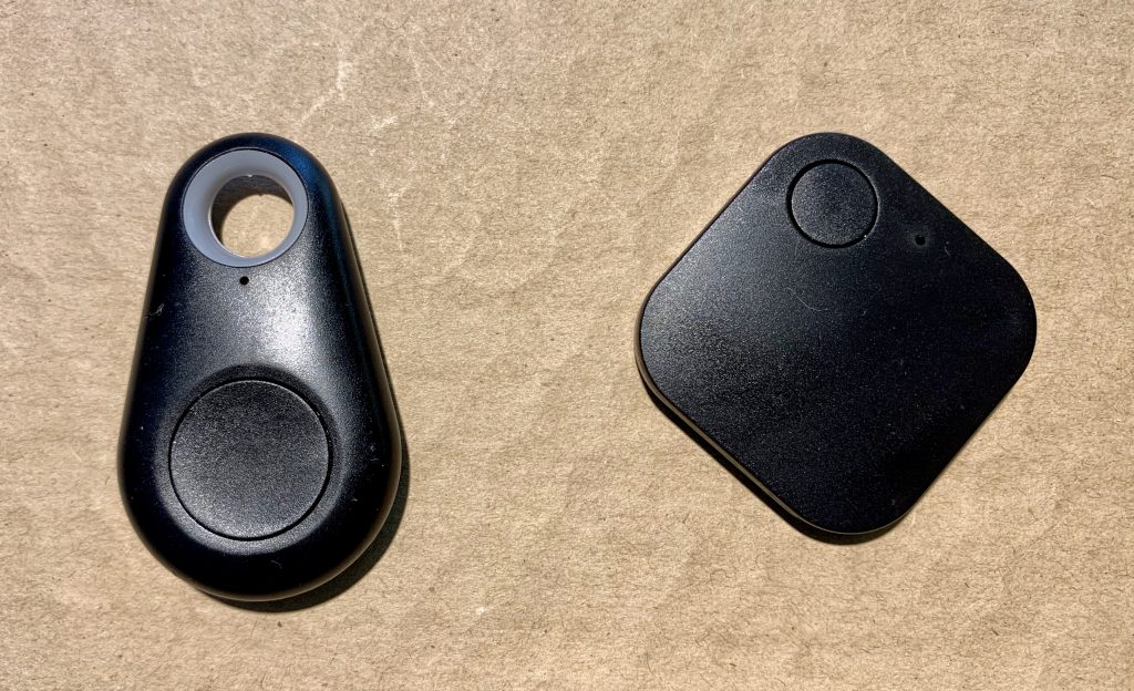
Some research into the present and near-future state of indoor locating technology led me, inevitably, to Bluetooth Low Energy (BLE) beacons. Bluetooth Low Energy led me, inevitably, into a short digression into Bluetooth “tags” for finding lost items like keys.
I just received a couple such tags I ordered from AliExpress for less than two dollars, each, and I made a video showing what’s inside when you open them up.
Yeah, I misspelled “bauble” in the title sequence.
These Bluetooth tags for finding lost items appeared on the market at about the time that Bluetooth Low Energy (Bt 4) started appearing in the latest smartphones. I don’t know who was first on the market, though I’ve seen the suggestion that the idea may have originally come from Nordic Semiconductor, one of the biggest companies dedicated to making chips for low-powered RF applications. I do know that Tile is probably the dominant vendor at this point.
The basic Bluetooth key finder “tag” is a small device, the size a condom packet, or a matchbook that can be carried on a keychain. Inside there is a small circuit board with a Bluetooth SoC (system on chip), a microswitch, battery, a pezioelectric speaker, and a few supporting components.
When it is powered on, the tag transmits to “advertise” itself. When it is advertising itself, a companion app, running on a smartphone can detect it and connect to it.
Once connected, the app periodically checks the signal strength of the tag. If the signal drops below a preset threshold, or is lost entirely, the app will notify the user, allowing them to stop what they are doing and find the object before they become too far separated from each other. The tag may start “chirping” automatically to make it easier to find. If the user needs help finding the tag while still nearby they can also use the app to instruct the tag to start chirping.
The system also works in the opposite direction. If the user is carrying the tag on a keychain in their pocket or purse, then the automatic chirping will warn them that they’ve become separated from their phone. If they realize they can’t find their phone when they are still nearby, they can also push the button on the tag to trigger a sound on the phone in order to make the phone easier to locate.
This basic functionality seems enough to be useful to people who loose track of things a lot. At this point, its available for less than $2, if one knows where to shop. For that price, one gets a functional but crummy app. The app may have added functionality, like the ability to use GPS to map the location where the phone was last able to communicate with the tag. This could be useful to determine you left your keys at the gym, rather than the office.
Tile, and others have gone further, in order to justify charging $20, rather than $2, and also to enhance their competitive position. If you use one of Tile’s tags, then, if your tag and your phone become separated, Tile’s app, working with their backend system, can check to see if any other Tile user’s phones “see” your tag, and then let you know where.
This tag-finding network sounds clever, but I wonder how well it works, and how useful it really is, particularly given the potential privacy concerns. It’s certainly possible to implement in a way that preserves privacy. In fact, Apple recently described the outlines of one such system they are developing to help people find lost or stolen Apple devices, extending their “Find My” app from iPhones to Apple Bluetooth devices, like AirPods, and also beyond WiFi range for Macintosh computers.
Apple is also rumored to be working on their own Bluetooth tag to allow keys and other objects to be tracked by the system. This might explain why Tile has recently partnered with a number of Bluetooth silicon makers, including Nordic, to extend the Tile network to third-party devices.
Back to the $2 tags I took apart, a few things of note:
The first has a teardrop-shaped case. The printed instructions point to the cTracing app. It shows up as “ITAG” using a general purpose bluetooth scanning app. Inside, I found a model XTR-FTQ-3432 PCB with V1.2, dated in 20181105. The SoC is from a Shanghai design house called Beken, and the part is BK3431.
Back in 2015, Brian Khuu tore down a tag that used the same case. His tag came, packaged for retail, in a box labeled iTag. Inside he found a different IC, labeled as ST17H25. One of the commenters identified it as a Telink TLSR8266 F512. It is actually a Lenze ST17H25. The two are quite similar, down to the names of the authors associated with revisions of the datasheet. It’s a bit overkill for this application, with a 14-bit ADC and, microphone input.
In any case, they’ve switched to a different SoC now. The BK3431 has a more limited I/O, making it more similar to the Lenze ST17H26, which is what I found in the second tag.
The second tag’s case has the shape of a rounded off square. There is a slot that a small lanyard can be looped through. Inside, it looks very much like the device pictured in this teardown on the Simply Soldered blog, which also uses the ST17H26 on a model RB-FD02 PCB. There have been some changes since then, though I’m not sure what they are. The PCB in my devices is V1.9, dated 20180606, the earlier teardown shows PCB V1.2, dated 20151212. I see some differences in component placement around the crystal and the antenna. I don’t know about accompanying differences in the schematic and if I took the time to check, and found some, I wouldn’t know the significance.
A couple of years ago I bought a Ravpower 30W USB PD powerbank with one USB Type-C port, and two regular 5v USB ports.
It was a little quirky. Sometimes it would start charging itself from the laptop until I held the button down for 5s. At some point the behavior started getting worse, to the point that last summer I left a poor review. The seller contacted me quickly, and I had a replacement within a week. The replacement fixed the problem.
That left me with the defective unit. Today, I decided to take it apart and see what’s inside.
Regulation of voltage and current for lithium ion battery charging for 1s-6s battery packs (4.2-25.2v)
Charging current to 10A!
Input voltage from 2.7-30v
Output to load from 2-30v & 60W
The pack sells for ~$75. To put things in perspective, you can buy eight FL1 cells for $4.41/each, which works out to about $35. That price drops to $3.56 each through a grey-market seller if you buy a thousand at a time. Ravpower is almost certainly paying less than that.
You can see more in the YouTube video I shot of the process:
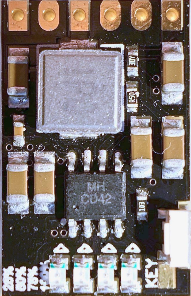
This module, like the MH-CD42 module I looked at recently, has a single IC with unhelpful markings. Since the IC on that board appears to be from Injoinic Technology, I thought the IC on this module might share the same origin.
I reviewed the product offerings on their English language site and thought the ICs for car chargers looked the most promising. Based on the summary specifications, the IP6505 fills the bill. This IP6505-based module certainly carries the same supporting components, and the IC shares the same footprint.
The IC combines an efficient synchronous buck converter and logic for negotiating power delivery using a variety of USB charging protocols. My primary interest is in Apple 2.4A/12W charging, but it also supports Qualcomm’s QC2 & QC3 protocols, which is popular among android smartphones using Qualcomm’s SoCs.
I see that their IP6518 IC, which supports 45W USB PD charging is available on inexpensive modules, too.
I just received a USB / LiIon power module I paid ~$2, including shipping, for on AliExpress. The model is given as MH-CD32 (link goes to what I think is the original manufacturer, though I purchased it from another seller with cheaper shipping).
The board is supposed to be an all-in-one solution for powering a 5v (ie USB powered) device from a lithium ion battery pack. I suspect the IC was originally designed for use in a USB powerbank. The basic features are:
Charging of 3.7v nominal, 4.2v max, lithium ion batteries.
5v charging input, 2.1A max charing current
Battery protection for over current, over voltage and over temperature (for the charging IC, at least, there is no provision for a thermistor to sense pack temperature)
5v output, up to 2.1A
4-level battery “fuel gauge”
Power path management: when the module is externally powered, it can power the load and charge the battery with any excess power from the supply.
Control input that can switch the output on, or off, suitable for control by a microcontroller.
100uA quiescent current.
It accomplishes this all with a single 8-pin IC, a dozen discrete passives (an inductor, eight ceramic capacitors, three resistors), four LEDs and a microswitch. All in all, it looks like a useful module.
I’m curious about what IC it uses. The package has markings, but they aren’t useful; it’s marked MH CD42, which is the model number of the module. Nothing strange about that, except that Google searches don’t turn up anything, no Chinese datasheets, just more product listings for the module.
Ordinarily, the first couple of letters of a chip marking echo the name of the manufacturer, but in this case, they instead they echo the name of the module manufacturer “MH-ET.” It isn’t uncommon that manufacturers “sand” the IC package to obscure it’s origin. In this case though, it seems that MH-ET has either remarked the chips or, more likely, had the packages custom marked.
If I were a competitor, and this were a product that had some combination of a large market, a high margin and a high selling price, I could go to great lengths to discover the true origin of the integrated circuit. I’d start by gathering the basic details of the product and using that to infer the specs of the IC. There isn’t much guess work in this case, because the product is a manifestation of the the capabilities of the IC, and its typical for the sellers to use the ICs specs when describing the module, even when the implementation cuts corners that may compromise the specs.
I’d use the specs I gathered to search catalogs and databases for similar ICs and compile a list of candidates. If my goal is to produce a competitive product in terms of cost and capabilites, I’d investigate pricing of the candidates and if any of them met the functional and cost requirements, that might be the end of it.
If I couldn’t find an equivalent chip, or if I wanted to improve my negotiating postion, or if I was involved in making or selling a competing IC, I’d dig deeper. I’d look more closely at the details of the IC, the specific package, the functions of each pin, the details of the circuit connected to each pin and I’d compare them to the documentation available for candidates I’d previously identified based on basic specifications.
Beyond that, I could order samples of the candidates and test their behavior against that of that of samples of the unknown chip. Or, perhaps I’d use chemical or mechanical means to extract the silicon ship from the enclosing package and then examine it under a microscope before and after stripping away layers of metalization on the IC. This might show me markings like a date code, part number, or logo. It would certainly show me the gross and fine structure of the circult. All of them would help me find the true origin of the integrated circuit.
I’m not going to do that though, in fact, I’ve already spent more time writing about it than I’d like to spend on what I am going to do.
Rather than going to those lengths, I’m going to take a shortcut that I happen to have available to me: I remember seeing a similar module on eBay a few months ago and I remember that the IC on that module had a distinct an unfamiliar manufactuer logo on it.
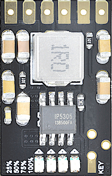
It took a little longer than I expected, but I found the ebay listing, or one like it. There IC lacks a distinctinve logo, but it does have a clear part number “IP5306,” and that part number leads to a catalog listing on a distributor’s site, a datasheet and the manufactuer, a company called Injoinic Technology.
The PCB layouts are very similar. The IC pinouts seem identical. I tried tracing out the circuit, but I could only get so far without removing components. The only real question are pins 6 & 7.
My 4.5 digit multimeter shows ~0Ohms resistance between them, suggesting they are on the same node of the circuit. However, if the IC on my MH CD42 board is the same or equivalent to the one on the IP5306, then those pins should actually be on two separate nodes of the circuit. Pin 7, on the left, should be connected directly to the near side of the inductor, while pin 6 should be connected to the far side of the inductor, by way of the low-value 500mOhm resistor you can see in the photograph.
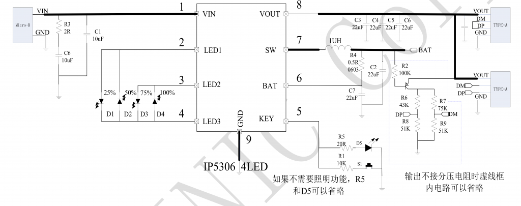
IP5306 Typical Application Circuit
It wouldn’t be hard to pull off some components and replace them later, or it shouldn’t be, but I always seem to hit a snag on the easy jobs, like loosing a tiny component, or delaminating part of a trace. Fortunately, I have a nice Keithley 2000 6.5 Digit DMM. It’s serious overkill for most stuff, and measuring miliohms isn’t its forte, but it only took 30s to boot up (it actually has a Motorola 68030 process, like an old Mac ][, or SE/30 computer), and less time than that to show that the path from Pin 6 to Vbatt had 500mOhm higher resistance than the path from Pin 7.
So, my conclusion is that the MH CD42 IC is actually an Injoinic Technology IP5306. It’s possible that it is a “clone,” or that they both actually come from a third party, or are otherwise derived from the masks and foundry. It may also be true that there is another IC on the market that defined the specs and pinout and that a very narrow market niche has emerged around it. I already know more than I need to know, and if you’ve read this far, then you know it, too.
I’ve been researching indoor location technoglogy which has lead me to looking more closely at the cost and effort of implementing Bluetooth Beacons, like Apple’s iBeacon or Google’s now unsupported Eddystone protocol. That led me to Bluetooth “Trackers,” “Tags” or “Key Finders.” There are also BLE sensor tags and fitness trackers. These are my barely edited notes.
Cheap Modules
There are a huge number of cheap Bluetooth ≥4 modules on eBay and AliExpress. Some are bare modules that include a Bluetooth SoC, an antenna, and supporting circuitry intended for integration into a larger device. Others are, more or less, finished devices. The have cases, and battery holders or connectors for an external USB power supply. They also often have demo firmware and apps.
Tracker devices are available for less than $2, with shipping, but they have unknown or poorly documented SoCs and repurposing them may be difficult or impossible.
For more flexible modules with well documented and supported SoCs from Nordic and TI, prices start at $4 for a basic coin cell powered device with Bluetooth 4LE support and go upward for more recent chips with support for later Bluetooth version and/or cases for more durable installation. Bare modules for incorporation into devices are available for less than $2.
Shenzen Wellicorp: fixed and portable beacons with waterproof housings using nRF51, nRF52 and TI CC2541 SoCs.
Bejing Aprilbrother: DA14580, nRF52 & TI based fixed and portable beacons and sensors.
Holyiot Sensors and beacons based on nRF51 & nrRF51. Also
Minew sensors, beacons and electronic shelf lables based on nRF51 & nRF52 and, TI BLE SoCs. Their beacons were used for Google’s first public Eddystone demo. They sell BLE 5 capable beacons for $10 + shipping, with a three unit minimum order.
Bluetooth Profiles of Interest
Proximity
Find Me
Common Bluetooth SoCs
Their are a variety of manufacturers of Bluetooth SoC, but Texas Instruments and Nordic Semiconductor seem the most common.
Is there any standardization of a protocol for configuring beacons?
Bt 5 Advertising Enhancements — Use of more channels for advertising packets, reducing interference. Extended advertising lets advertisements use a larger payload (in another channel), allowing more info to be conveyed in beacon applications.
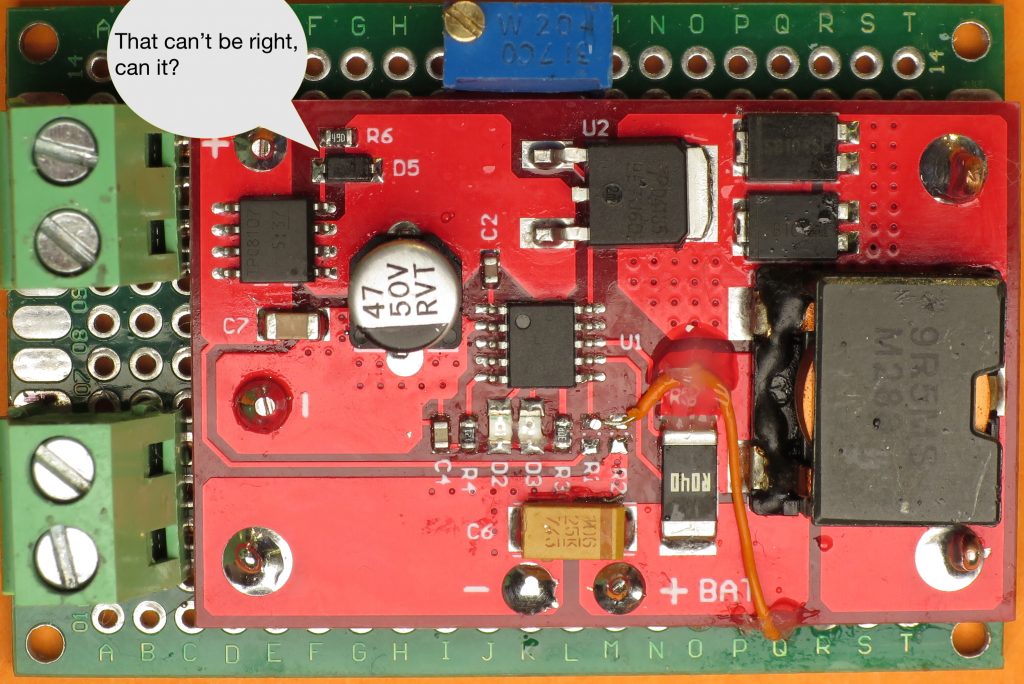
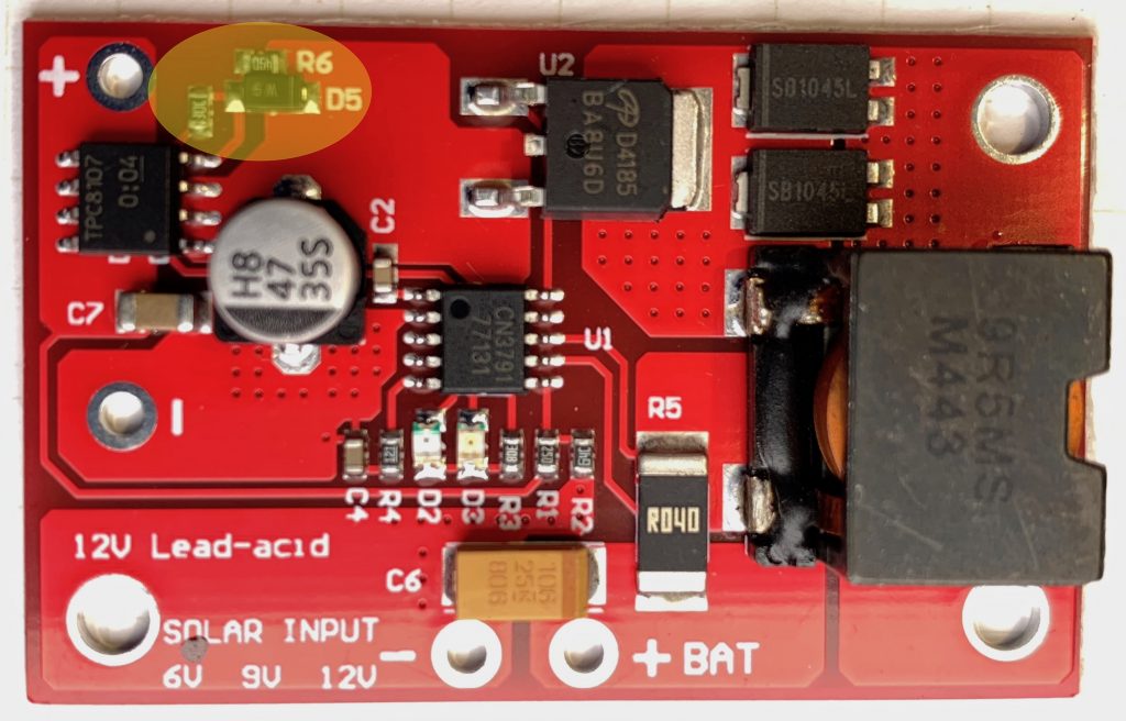
Last year, I paid about $3.66, with shipping, for this solar-powered MPPT lithium ion battery charging module on eBay to use with my small solar panels and scavenged 18650 batteries. It has some issues.
First off, the version I purchased/received is intended for 9v solar panels and I wanted to use it with a ~6v panel. This is set with a resistor divider. Careful study of photos from product listings showed that the divider was implemented using the same resistor value for the high segment of the divider, changing only the value of the lower segment’s resistor to change the setpoint.
The high segment had a value of 178KOhm and the low ranged from ~42KOhm for a 6v panel down to 12.6KOhm for an 18V panel. I didn’t have any SMD resistors of suitable value in my supplies, and I couldn’t find any I could scavenge on any surplus PCBs. I decided to use a trimpot instead. I had a variety on hand, and it would allow me to experiment on the optimal clamping voltage for the panel I had on hand, and an 18V panel I’d ordered. I chose a 200KOhm trim pot with the idea that approximating the total resistance of the existing divider would help preserve the stability of the control loop. If I were going to do it again, I’d probably choose a different configuration to minimize the impact of the pot’s temperature sensitivity. A simple choice would be ~20KOhm trimpot, configured as a variable resistor (short the wiper to one terminal) used it to replace the low segment, leaving the 178KOhm resistor in place.
After adding the potentiometer, I connected the battery and panel and adjusted the potentiometer until I maximized the charging current. I was a little surprised by how low the panel voltage was, and so I started poking around. The first thing I checked was the voltage drop across a P-Channel MOSFET on the panel input. I was surprised to find that it was 500mV, though knowing that, I wasn’t surprised the IC was noticeably warm. The panel was dissipating 1/10th of the panel voltage over the MOSFET!
Some of the photos on some of the product listings showed a simpler circuit, without anything in the panel input current path. My guess is that the MOSFET and accompanying resistor and diode were added in a revision in order to protect the circuit in case the panel polarity was accidentally reversed, and/or to block leakage of charge from battery through panel at night. A schottky diode would accomplish the same thing more simply, but with a voltage drop of ~300mV. Properly implemented, a MOSFET based “ideal diode” would have an effective resistance of ≥ 50mOhm, and a voltage drop of ≥ 50mV at the ~1A max current my panel could deliver.
I’m not completely sure how the circuit was intended to work, but clearly, it wasn’t doing the job. I wondered if it would work properly if I was using the module with a 9V manual, as intended, but that didn’t seem possible, either. The panel + was connected to the MOSFET’s source, the rest of the circuit to the drain, and the gate was connected to the drain via a resistor and diode. By my reasoning:
that the gate would ≅the potential of the drain
the voltage drop from source to drain should be as close to 0V as possible in order to maintain the efficiency of the curcuit
therefore, Vgs would/should approximate 0V
but it won’t because the Vgs threshold for the MOSFET was ~2V!
I wasn’t sure how to fix the circuit, but I was sure that the gate needed to be pulled down to a lower voltage, so I cut the trace connecting the resistor the drain and connected it to ground instead. It worked well enough that the voltage drop over the input MOSFET went from 0.5V to a trivial number. I’m pretty sure though that I didn’t fix the protection function.
I’ve since received another version of the module which has revised the input circuit. The diode and parallel resistor connecting the gate and drain are still used, but there as another resistor which connects to the charging indication pin on the CN3791, and in so doing. This pin is open drain. When the battery is charging, it is pulled low, lighting the charge indicator LED AND pulling the input MOSFET gate low. Vgs ≅ -Vpanel ≅ Vs ≅-6V, turning the MOSFET fully on.
Thinking through this further… if the battery is charged and the panel is illuminated the gate will approximate the potential of the input MOSFET drain and, since the only load on the panel is the quiescent current of the module, then Vsd ≅ 0V ≅ Vgs and so the MOSFET will be off, save any current through the body diode.
If the panel is dark and the battery is charged then Vd of the input MOSFET will, at most, be at battery voltage (Vbatt), Vs will be ~0v, Vg will ≅ Vd, Vgs ≅ Vd and the input MOSFET will be off.
If the panel is reversed Vs will be below GND and well below Vg ≅ Vd ≅ Vbatt so Vgs will be Vbatt + Vpanel, and the MOSFET will be off. Note: This means that reverse polarity with an ~18V nominal panel would exceed the Vgs maximum of 20V for the TPC8107 MOSFET used at the input.
If I get around to it I’ll draw a schematic and add it to this post.
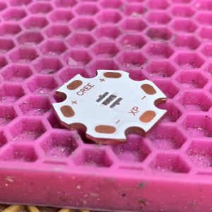
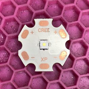
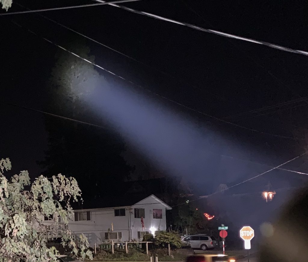
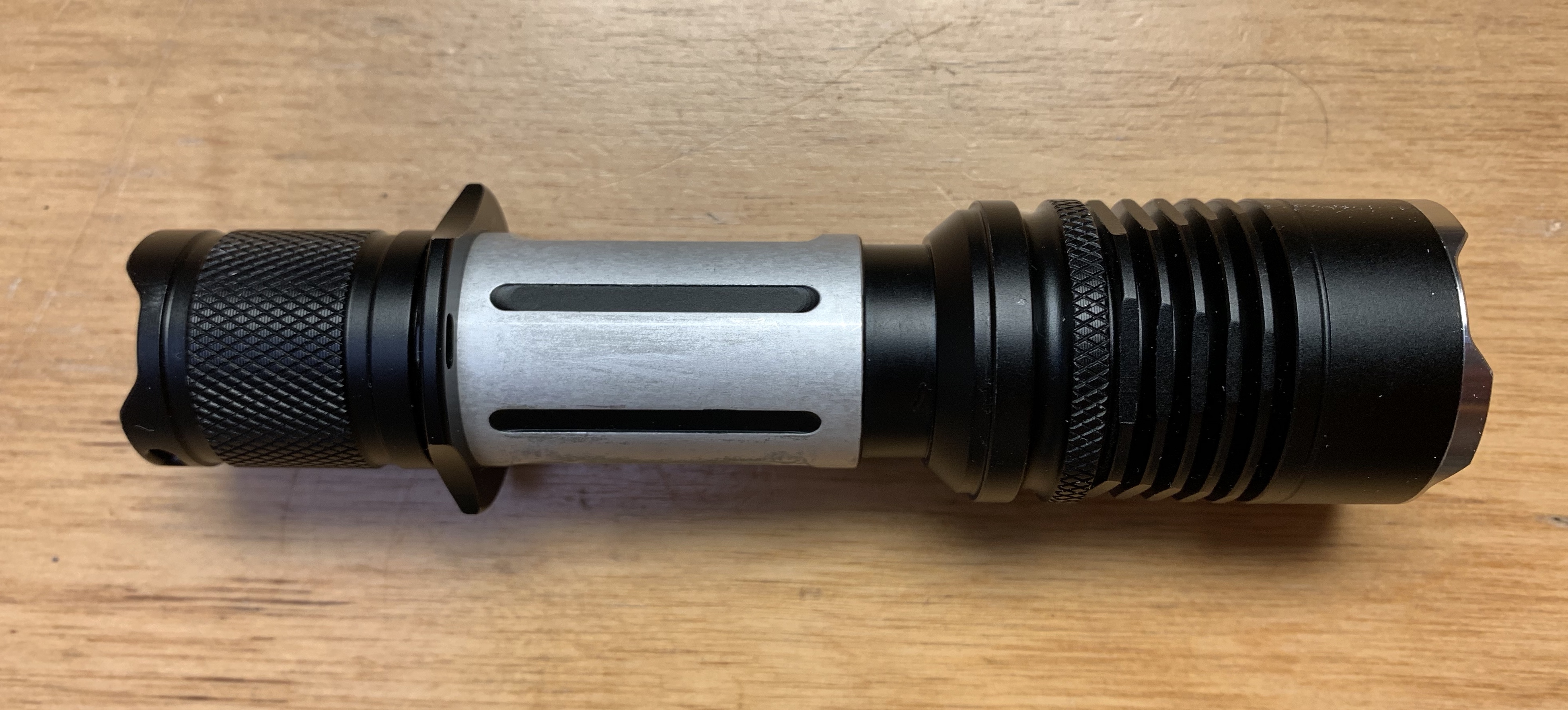
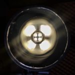
Last week I received some OSRAM KW CSLNM1.TG emitters (aka the “White Flat”). These are dome-less, small die (1x1mm) LEDs. Today I installed the first one in a VG-10 style flashlight. The results are impressive.
Stencil FTW
I don’t have good beam shots, yet, but I can say that the hotspot is slight larger than the hotspot from a Convoy L2 with an XPL-HI emitter. Not bad for a light with a 23mm reflector.
Update: I measured the hotspots of this light, and my L2. The diameter of this light’s hotspot is about 1.25x that of the L2, so it has 1.5x larger area.
Poor quality beamshot. Also the automatic HDR on newer iPhones is crazy.
I’m currently running it off a 3 amp buck driver, so it’s isn’t putting out as many lumens as the XP-L HI in the L2. As a result, the intensity is lower. I plan on upgrading the driver soon to push it up to ~5A or so, at which point the output and throw should rival that of the L2.
These emitters have a 3x3mm package. They work pretty well on a standard XP footprint (3.5×3.5mm), but they don’t work so well with XP centering rings. I ended up using a modified XP centering ring. I placed it on a drop of UV set resin and then lifted out slowly so a thick film was left across the opening. I then “popped” that film so that the resin clung to the edges of the whole. I hardened it with UV light, then opened the hole up with a small triangular file until I had a centered opening that fit the emitter. It came out pretty well and the focus isn’t bad either, though I’ll probably try and adjust it further when I open the light up again for a driver upgrade.
I have two more of these emitters. Next step is to put one of them in a C8. I’m not sure what to do with the last one. I’ll probably put in in the L2.
Stripped to conceal poor removal of ugly “Forfar” logo. I like it. Protip: UV set resin makes a nice & precise resist.
I wanted a solder paste stencil to make it quick and easy to reflow emitters onto Noctigon 4XP 33mm MCPCB used in the Emisar D4S flashlight. I made a gerber file that I used to cut a stencil out of polyester sheet using a craft vinyl cutter.
Most flashlight hobbyists don’t bother using a solder paste stencil when reflowing emitters. They just slop some solder paste onto the MCPCB thin it out a bit, put the emitter on and then heat the MCPCB until the solder paste melts. Then they wiggle the emitter around to make sure the solder is evenly distributed. Finally, they give the emitter a “bonk” to eject excess solder and let it cool.
I’ve used the slop & bonk method before with decent results, but its a little to fussy and inconsistent for my tastes. It’s workable for single emitter boards, but with triples and quads, trying to manage the inconsistency leads to more fussiness which leads to the emitters being heated longer, which can reduce their efficacy.
Solder paste stencils reduce variability and fussiness. They make it easy to apply a precise amount of paste evenly, which makes it practical to reflow emitters with little or no manipulation during the molten solder phase.
I’m sharing the gerber file in case anyone else has access to a suitable cutting plotter and wants to make their own. I used the open source Gerber2Graphtec software to convert the gerber into a file that I can send to Silhouette Cameo 2 cutter. This software only works with Graphtec-based plotters, like the Silhouette family.
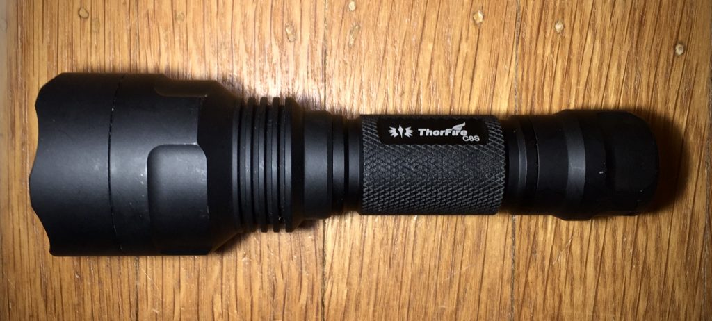
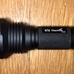
I’ve been looking for an inexpensive way to build a compact, high-output (>2500lm) flashlight. This post documents a successful result.
There are two straightforward routes to a high-output flashlight. The first is to use a high-output emitters like the Cree XHP70.2. The second is to use multiple (often three or four) lower output emitters.
The downside of high-output emitters is a combination of expense and limited choices for both driver and emitter. The emitters themselves aren’t badly priced when considering power/$, but they typically require a 6v power-source, which requires either a high powered boost driver, or two batteries in series, requiring a larger host. In addition, there are fewer choices for CCT, tint, and high-CRI among high-power emitters.
Multi-emitter configurations are commonly configured with the emitters in parallel, meaning they can be powered with a single cell controlled by a wide-range of drivers. In addition, they can most of the 3v emitters on the market, in any combination your heart desires. The downside is that they generally require specialized MCPCBs, which must be pared with optics or reflectors with matching spacing. These reflectors and optics are shorter than the single reflectors most hosts are built for, so they either need custom spacers, or a specially built host.
My project has the advantage of working in a variety of single-emitter hosts with minimal modifications, while allowing the use of 3v drivers and a wide array of emitters.
Ingredients:
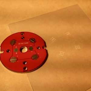
One Thorfire C8s
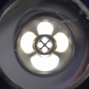
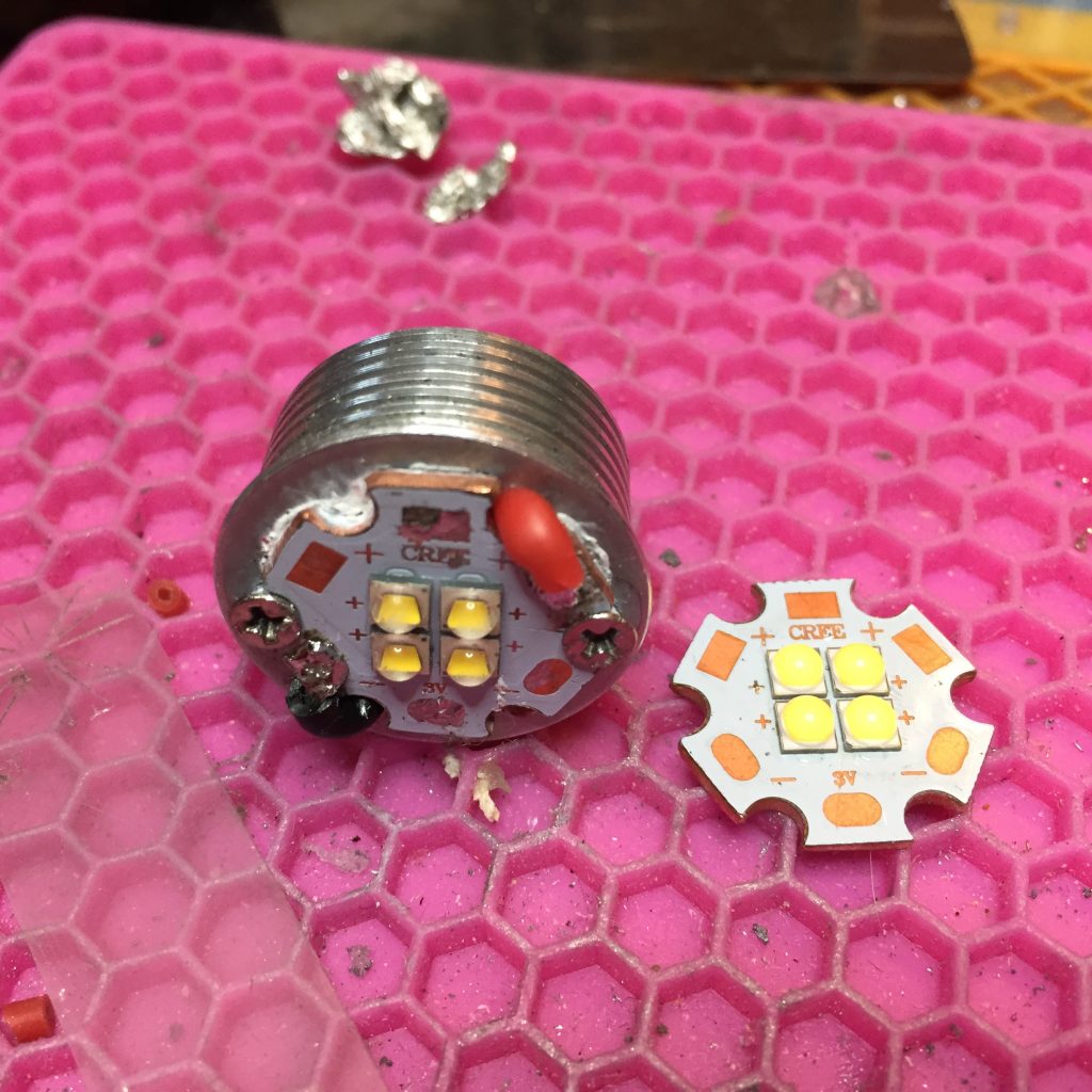
Four warm white XP-G2 of unknown flux binning…
Mounted in a 2×2 array on a direct thermal path copper MCPCB which electrically connected them in parallel
DCfix diffusion film
Lexel’s 17mm version of the TA v1 driver.
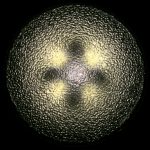
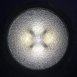
For my first pass, I used an orange peel reflector I had on hand in the hope that it would, on its own, blend the beam enough to eliminate a dark spot in the center caused by the gaps between the emitters.
When that didn’t work, I used some diffusion film, which worked really well, well enough that I decided to try the original reflector. The film was still enough to blend the beam enough to remove the dark spot in the center of the beam.
The end result is bright and quite floody. I don’t have a great way to measure the brightess or intesity, but I’d guess that its less bright than my BLF Q8 and brighter than the 3x Nichia 319a emiters I put into a Sofirn C8F
I still have more of the MCPCBs, I’d like to try another build, but I’m not sue what emitters to use. I want more power, and also higher CRI.
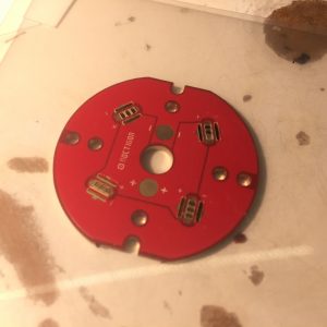
Update 2018-09-02:
I got a UNI-T UT201-E clamp meter last week and rigged up a modified tail board so I can measure the current draw of flashlights. I wanted to approximate the electrical characteristics of an actual flashlight, so I used a standard tail-switch board, with a bypassed tailspring. I attatched 13AWG wire so I have a loop I can use to measure the current with the clamp meeter. I also put a standard Omten 1288 switch in line, to reproduce switch resistance. With fully charged, high-drain cells, I got a peak of about 11A. Not bad, but I wanted more.
After studying datasheets and independent tests, I decided to use some 90 CRI Samsung LH351D emitters I bought recently. By my estimates, they’d peak at ~4A each (16A) total, and produce a peak of ~1200lm each, for a total of 4800 lumens, peak (out the front lumens will be lower). Not bad for a 90CRI light.
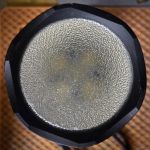
I have 5000K emitters (PN: SPHWHTL3DA0GF4RTS6) and 4000K emitters (PN unknown). I decided to use two of each. I reflowed them on to an empty 2×2 emitter MCPCB that I’d lapped for better contact with the emitter shelf. Once I had the light back together, I did more tests.
XP-G2 (left), LH351D (right)
I’m happy to say, my estimates were pretty good. With a Sony VTC5A, the peak current draw was over 18A. With Samsung 30Q or LG HG2, the peak current was ~17A. I don’t have way to measure output, but I’d assume those numbers are on track too.
Not surprisingly, the light heats up very quickly on full power.
~4′ from surface
~8″ from surface
To give some sense of beam uniformity, I took a couple shots at different distances against blank surfaces. Don’t compare the color between shots, the surfaces are different shades of off-white, but the color uniformity in each shot should be useful.